This image from wikipedia, explains that there occurs a potential drop across a pn semiconductor junction, and an electric field confined to the depletion region.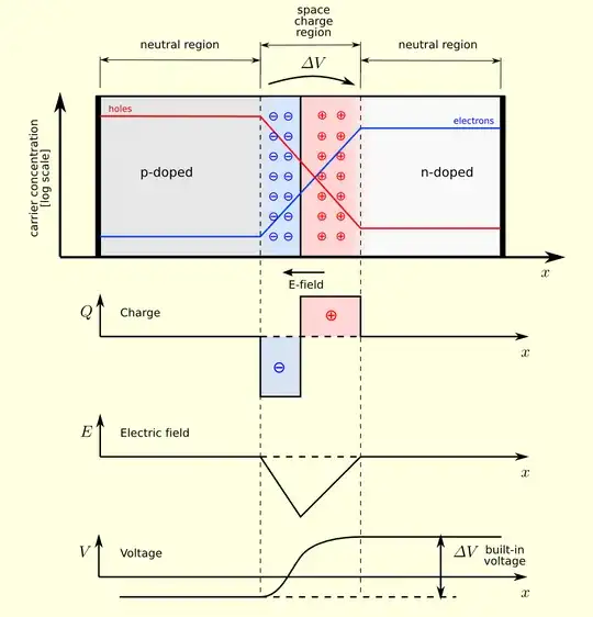
I already know the reason for the existence of this drop and the calculation of the difference but I have two questions regarding this drop.
1) If the n and p doped regions are externally connected using a perfectly conducting wire, why will not any current flow?
Connecting the two regions should equalize their potentials (since wire is a resistance less) conductor, and therefore the gradient at the junction is destroyed resulting in a diffusion current which is obviously against conservation of energy as the semiconductor has non-zero resistivity. Where will extra potential drops will be created so that Kirchoff's voltage rule holds without any current and the built-in potential difference $V_o$ of the juction persists?
2) (probably naive) If an external Bias is applied, of say $|V|<|V_o|$, then the pn potential difference across the junction will just reduce by that amount ($|V|$). Assuming that the external voltage source is ideal without any resistance, what will be the potential drops which would sum to zero in this case? Will drop due to the resistance of semiconductor play a par in it? If yes, then there cannot be any ideal resistance-less semiconductor junction, can there?