What is the quantum mechanical model/description for excitation of systems via application of electric power/current? Consider for example your display that you look at while you read this. The system is clearly excited by the application of electric power which leads to luminescence. Usually we treat transitions induced by photons but how are systems promoted to an excited state when electric power via a current is applied? Can we induce specific transitions or is this a "thermodynamic" process where states get populated according to a Boltzmann distribution? What is the model for this process within quantum mechanics?
1 Answers
Quantum transport is essentially non-equilibrium
Let me first note that quantum transport is a vast subject, covered in many books using a variety of approaches. Quantum electrons are accelerated by electric field just like classical ones, as we can easily see by writing operator (Heisenberg) equations of motion for Hamiltonian:
$$
H=\frac{p^2}{2m}-eEx\Rightarrow\\
\dot{x}=\frac{1}{i\hbar}[x,H]=\frac{p}{m},\\
\dot{p}=\frac{1}{i\hbar}[p,H]=eE
$$
However, this immediately takes us beyond the textbook QM, since we either have to deal with an unbounded spectrum or consider a more realistic situation, where electron gains energy via being accelerated by electric field, but loses it via collisions with the lattices, and emitting phonons, photons, etc.
In other words, quantum transport requires simultaneous application of quantum mechanics and non-equilibrium statistical physics (which is probably what is meant as "thermodynamic" in the Q.)
Nanoscale world is different
Thus, we are forced to look into details of what is happening to electron in quantum regime - e.g., by tretaing in details electron-phonon and electron-photon interactions... the problem is that such phenomena are typically studied in nanoscale devices, where things happen in ways very different from our high-school picture of electrons accelerated by a constant electric field through a wire - we have now weak localization, conductance quantization, QUantum Hall and more odd stiff. This then requires a totally different view/description of how electrons behave in quantum regime.
Quasiclassical approach
Going back to an electron accelerated by electric field, the above cited equations of motion form the basis of the simplest Drude-like description of electron behavior in bulk materials, which can be found in basic texts like Ashkroft&Mermin. This is essentially writing a Newton equation for electron with viscous friction:
$$
\hbar \dot{k}=-\frac{\hbar k}{\tau}+eE,
$$
where $k$ is the Bloch wave vector in a band.
From this we obtain stationary velocity
$$
v=\frac{\hbar k}{m}=\frac{eE\tau}{m},
$$
and multiplying this by electron concentrations and charge we arrive at Drude conductivity.
This turns out a surprizingly versatile approach, see, e.g.:
Heating effect of electric current
How is absorption integrated in the simple Drude model?
A notably simple generalization of this approach is to replace viscous friction by energy losses occurring at random instants distributed according to exponential law - as in the famous superlattice paper by Esaki&Tsu.
A significantly more advance version of this approach is Quantum kinetic equation, which is a systematic perturbative amelioration of classical kinetic equation - discussed in details by Rammer&Smith.
Quantum junctions
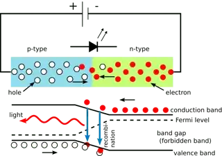
One important thing to mention is that kinetic equation needs to be solved self-consistently - that is, accounting for the electric field created by the moving electrons themselves, which modify the electric potential within the device (in other words, we need to account for screening... but in non-equilibrium situation.) In quantum devices that forces us to completely rethink the way we describe a device to which electric potential is applied. The classical description of semiconductor devices is thus that of a p-region and n-region with constant chemical potentials (in these regions the potential is screened), the potential sharply dropping on the junction (image source):

The effect of the potential difference is then simply changing the difference between the chemical potential between the two sides of the junction. The electrons then move from one part of the junction to the other by recombining in on the border between the two regions. Note that this is a quantum description of electric current - even if it looks very different from what our classical intuition of electrons accelerated by the electric field suggests.
Note that LCD screen, cited as an example in the Q., functions differently - it contains elements that change transparency when a bias is applied to them, and which are highlighted by an independent light-source. That is, there is no really direct conversion of electric power to the luminescence.
Landauer-Büttiker approach
For more complex nanostruictures, where electrons can actually move without scattering on significant distances ("ballistic regime") a special method of calculation was developed by Landauer and Büttiker. This method is used for treating phenomena such as ballistic conductance (which is not infinite, contrary to classical expectations), conductance quantization, quantum Hall effect, transport through quantum dots, etc.
The essence of this approach is that the bias still falls onto the central region of the structure, and is completely screened in the leads/wires connected to it. The electrons are then injected into the eigenstates on one side of teh structure, evolve in completely quantum way, and then recovered on the other side of the structure. In simplest cases the resistance of the structure can be simply expressed in terms of its scattering matrix - the same as in QM tests or QFT books.
These methods are well covered in Joe Imry's book.
A good summary of different approaches can be found, e.g., in Haug&Jauho or in the book by Supriyo Datta.
- 68,984