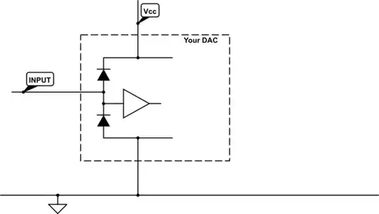
This is the most interesting thing I have seen! I have built a DDS that sends data (D0-D7) to a DAC (ADV2175). The design worked fine and I just have a low frequency alias noise (a question here). This noise was present on all my ground planes (This is in prototyping stage and that's not unexpected from the test PCB).
I started tracing the noise path by disconnecting wires to see when the noise is gone. Surprisingly even after disconnecting all VCC and GND connections (+ all VREF and logics gone to 0 or 1) the noise was present yet. The more unexpected behavior is when the DAC is just connected to DATA port+ CLK pin (all coming from the source FPGA, NO VCC or GND), it continues working and a sine wave is produced (but with the same noise)!!!
First I thought it may receive its VCC/GND form the logic 1/0 fed into it but if it was correct, it should not have produce 0x00 and 0xFF levels, but it makes those levels correctly (I changed 0xFF data stage to another level and a notch appeared on top of the waves. this shows it can build oxFF correctly).
This is a big challenge for my PCB design, as if this device really takes its GND from the data port, instead of the dedicated pins, I will have a hard time for designing a reliable ground plane for it (the return voltage should go back to a logic noisy environment and analog-digital ground plane isolation may be impossible).
Can anyone explain what is happening there?

