4

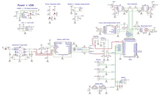
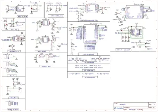
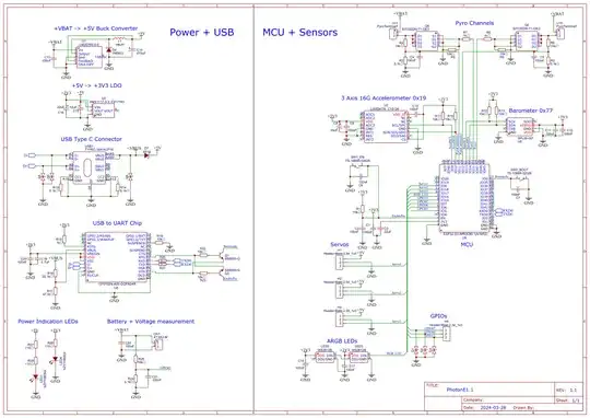
After reading all of your feedback on my flight controller schematic I posted two days ago in Model rocket flight controller schematic review, I redid the entire schematic and tried my best to make it readable and easy to understand, so that others can more effective look over it and check for errors/mistakes.

The main goal was to make connections clearer, and not so split.

Is my second version better, in terms of readability?

And what are things to improve? (mainly on the "aesthetic" side; not for the functional side of things)

This is the first version:

Enter image description here

And this is the new, second version:

Enter image description here

Peter Mortensen
  • 1,679
  • 3
  • 17
  • 23
Fazeli24
  • 97
  • 7
  • 3
    It seems that every component is producing junction points. This steps on my delectate sensibilities as when I see junction points, I expect at least 3 connections being made. When there are not 3 or more connections being made, then I suspect errant wires causing issues. This is likely all a post-traumatic stress response from my Altium days.... – Chris Knudsen Mar 29 '24 at 19:10
  • 1
    Hi, this actually helped a lot! I looked over all junction points and removed the unnecessary ones. And that way I found an unconnected GND, so very useful tip! – Fazeli24 Mar 29 '24 at 19:27
  • 1
    There are still both design issues and likely just schematic drawing accidents. They might be hard to spot because of the way you draw them. – Justme Mar 29 '24 at 19:52
  • 1
    @Justme hi, I am sorry, but I am not quite sure what you mean. Could you maybe be a bit more specific? :D – Fazeli24 Mar 29 '24 at 19:57
  • @Fazeli24 You said you will make a new question about functionality. I can't say how you should draw a better and more understandable schematics. We all have some way we best understand things, but still need to read schematics made by others with different ways, and e.g. make them beacuse company style or customer wants it drawn with their rules. There is no one true way of drawing schematics. Or even if there is a standard, then there might be multiple different standards, and people still won't make them purely by the standards. – Justme Mar 29 '24 at 20:06
  • I'm not familiar with that accelerometer, but the connection of C10 from Vdd_IO to 3.3 V seems incorrect. I'd expect the capacitor to go from the IC pin 1 to Ground, and possibly connect pin 1 to 3.3 V. – Peter Bennett Mar 29 '24 at 20:07
  • 3
    The schematic is missing "flow", and not conveying a design strategy, or intent. Typically one expects to see signal flow from left to right, top to bottom (but hey, not always). Preserving the wire/connection lines to show important point-to-point connectivity to illustrate intent. Reserve ports (on and off-sheet connectors) for the mundane bits (when you can), like power distribution, and LED's (The easy stuff to figure out). Yes, no rules are 100% as we are often asked to do the yet-to-be-possible, and we need to make certain design decisions.. – Chris Knudsen Mar 29 '24 at 20:10
  • @Justme okay, I understand, I was just a bit confused. I will open the new question. I know that everyone has their own style, and preferences, but I can definitely agree with others that my first schematic was very unreadable. – Fazeli24 Mar 29 '24 at 20:10
  • @PeterBennett yeah, you are absolutely right, that's not how it should be connected. A bit weird though, because an employee of ST Microelectronics looked over my schematic, and didn't find that problem. – Fazeli24 Mar 29 '24 at 20:24
  • 1
    @Fazeli24 Just to be sure, you got a chip vendor officially to check your circuit, or some random forum person paid to try to look helpful? – Justme Mar 29 '24 at 20:59
  • @Justme probably the later one, their profile said "ST employee", but that's it. Weird that they didn't find it, even if they are just paid to look helpful, they probably still had some schematic knowledge. – Fazeli24 Mar 29 '24 at 21:10
  • @Fazeli24 You can't really expect company employees to use their paid work hours for something that does not bring revenue to company. If you are a hobbyist and buy one chip, they might make less than $1 profit, and an a person paid $60/h can then spend less than one minute looking and your schematic and replying. Of course the public forum makes the info accessible for others too, so it becomes kind of knowledge base or FAQ or how to avoid common pitfalls so people can get examples and don't need to ask that much questions. Basically you contributed helping them to do their job cheaper. – Justme Mar 29 '24 at 21:34
  • 1
    Whichever GND symbol you use, it *always* points down. Do this one thing, and you are ahead of 90% of the innergoogle. – AnalogKid Mar 29 '24 at 21:58
  • @AnalogKid yeah, I have noticed that in my first schematic. Things like pull-down and pull-up make way more sense that way too. – Fazeli24 Mar 29 '24 at 22:11
  • 1
    As an encouragement, while there is always room to improve, both of these schematics are easier to read than many schematics made by professionals. – jpa Mar 30 '24 at 09:50
  • 1
    In 2018 Olin Lathrop posted this almost definitive "how to". || He probably covers it but I'm rushing so will just note - "Crossing lines never join, joining lines never cross". This is valuable when paper printed diagrams get old BUT is a valuable rule regardless. The dots then become useful but not essential and there is NEVER any doubt. || Your C14 & feedback pin connections are an example. Offsetting the two joining points makes it certain that these are joined. As in eg your D8 and Vbus lines which have this offset. Very valuable. – Russell McMahon Mar 30 '24 at 12:24
  • This is essentially a duplicate question BUT I suggest it is valuable to leave it open with the new answers - plus a link to https://electronics.stackexchange.com/q/28251/3288 – Russell McMahon Mar 30 '24 at 12:26

3 Answers3

6

It's definitely an improvement but, nothing beats having main flow from left to right unambiguously connected on one sheet: -

enter image description here

And, you can improve the above by moving TX and RX on the MCU to the left side and physically making a connection to where they are on the USB/UART chip. It's all about main signal flows and not breaking it up. I can see what the design does now.

Andy aka
  • 456,226
  • 28
  • 367
  • 807
  • Okay, thank you for your explanation. For now, I am satisfied with the overall look of the schematic, and try to focus more on making an actual PCB out of it, but once I have some more time (I currently have a deadline ), I will focus on improving my schematic drawing skills. – Fazeli24 Mar 29 '24 at 21:14
  • You have to think of the main flow. On the left is usb then comes the converter feeding rx and tx to the MCU. The MCU acts like a collection point for the sensors so, that stuff is better coming out the right side or top and bottom of the MCU. – Andy aka Mar 29 '24 at 21:19
  • should I do the same with my power flow too? E.g. I use a Buck converter to turn my battery voltage into 5V and then an LDO to turn that into 3.3V. – Fazeli24 Mar 29 '24 at 21:30
  • @Fazeli24 not absolutely necessary. Most folk can understand a net connection from the output of a 5 volt regulator being picked up in a separate part of the schematic by a 3.3 volt regulator but, having said that, a power flow from right to left is preferred and is nicer if the 3.3 and 5 volt regulators are next to each other. – Andy aka Mar 29 '24 at 22:18
5

An old post on this forum by Jonk outlines good practices for drawing schematics.
Your second schematic is OK, meaning it is readable with some difficulty, however, it needs some cleanup.

Some thoughts on what I see:

  • Schematic symbols and reference designators can be found in IEEE Std 315. It's best to use the standards. If your region has a different standard for drafting, use it.

  • When depicting transistors, use the proper symbol instead of a box. When others look at your schematic proper symbols are instantly recognizable. Don't make viewers do extra work parsing symbols. Modern schematic tools allow homogeneous and hetrogeneous parts.

  • The common symbol has "GND" along with it. This extraneous text adds to clutter. There are times to show labels with common symbols if you have multiple commons. Also, this looks like Altium with the non-standard common symbol with four horizontal lines (it should have three horizontal lines). For that reason, I use a triangle symbol in Altium and hide the "GND" text. The first schematic has ground symbols pointing upwards which is bad practice. You fixed that in the second schematic.

  • Q5 & Q6 has crowding with junction dots touching Q5 & Q6 which looks like there should be a pin on Q5 & Q6. This adds confusion. Also the PyroContinuityn nets split the resistor symbols (R8 & R9) from the labels. There is no need to do this as you have ample space to route the net around the resistors.

  • Be consistent in your labeling. Most of your symbols have the reference designation over the value (good). R8 & R9, and other parts, have the value over the reference designation. The reference designation and vale should line up. C15, C16, & Q6 are good examples of being sloppy. A schematic is also a work of art.

  • No need to include the omega symbol for the resistor values. It clutters up the schematic.

  • My personal preference is to have reference information horizontal. LED1 & LED2 are examples of vertical text which I don't like.

  • My personal preference is to use upper case text except for design notes. Easier to read when printed. I also use a mono-spaced font with no ambiguities (i.e., 1 l I are distinct). However, Altium doesn't handle non-default fonts well when using the built-in PDF printer (solution is to use a third party PDF printer).

  • My personal preference is to use as few pages as possible. Having a one page schematic as you do is wonderful. On more complicated schematics I'll group functionality per page. Example: core schematic on page 1, power supplies on page 2. Unfortunately, Altium schematic editor gets very slow when there are lots of parts/pins on a single page. My cure is to work on small parts of the design on a separate worksheet page, then move (copy/paste) the section to the final page. Other approaches to the program slowness are to have a 20+ page schematic which makes it hard to follow.

  • Be careful about color selection. Some colors don't have good contrast when printed.

  • Check for connection errors like CN1-1 going to +VBAT. It looks like you are missing a junction dot. The design rules may show this as an error when you transfer the design to PCB.

qrk
  • 9,494
  • 1
  • 7
  • 26
  • Woah, thanks a lot for these detailed tips! I honestly just used the LCSC symbols for my schematic, I kind of thought that the manufactures would follow these guidelines (e.g. the MOSFET), but I will now make sure that I will change/modify the symbol according to standards. I use the EasyEDA default GND symbol, and color scheme, I will see how I can change that. Luckily EasyEDA seems to be quite fast, although I probably have not enough parts to say that. – Fazeli24 Mar 29 '24 at 21:22
  • 1
    See also https://electronics.stackexchange.com/q/28251/3288 – Russell McMahon Mar 30 '24 at 12:25
2

This is already much better. I would put all the power related circuits together (VBAT, 5V, power LED etc), and the USB circuit together with the UART circuit. Either connected or, at least next to each other (but then it will be obvious that you will want to connect them). But it's already OK.

Now it depends what you intend to do with the schematic. And according to what you want to do, you may want to make a second schematic, in another way.

Here the schematic is useful to understand how the circuit functions, how pins receive signals and what signals do etc. That's fine for the theoretical concept. Now, when the schematic is to serve as a preliminary to board design, or to be used later to compare the PCB with the schematic to debug something, then you are going to face problems, maybe making mistakes, because the pins are not in their right physical order. It sometimes makes the schematic easier to draw and to read to invert the pin orders or to reset the pins in a random order. But when you use your schematic to remember what your board is doing, to compare it with the real PCB design, check the datasheet (where pins can also be put in random orders in some circuit examples, but not in the same random order as yours), then you will run into troubles and lose time.

A second schematic where pins are in their original order and where everything is connected could be useful prior to design the PCB. It will help you place and rotate the components already in a rational way, visually closer to the real PCB while still having all the informations about the circuitry. It's not possible to make a schematic identical to the PCB, because you always rotate or move something to reduce trace lengths and so on, but at least, you can have intuitive similarities. When, 5 years later, you will look at your PCB and at the schematic next to each other, you will remember what does what easily, and won't lose half an hour scratching your head.
Fredled
  • 2,310
  • 1
  • 10
  • 19
  • 1
    "where pins are in their original order and where everything is connected could be useful prior to design the PCB." For initial and prototyping runs, I highly encourage this (but I also often get some internet heat for suggesting it). When you're poking the probes around, trying to find that one poor decision, having an accurate representation of the physical parts can really help. – Chris Knudsen Mar 29 '24 at 20:53
  • Okay, thank you. After finishing this project(right now I have a deadline), I will work on my schematic drawing skills. When I start a new schematic, I will try to make 2 schematics, one for understanding the circuit function and one for debugging. – Fazeli24 Mar 29 '24 at 21:28