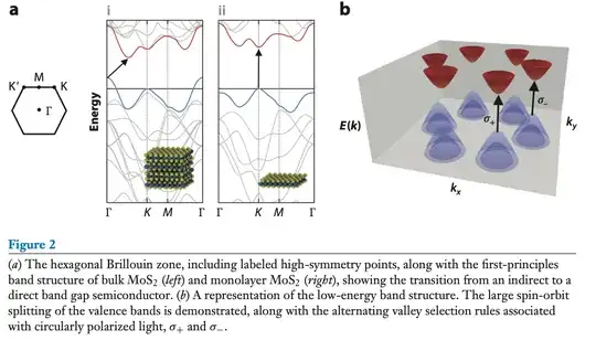
In the paper Optical and Excitonic Properties of Atomically Thin Transition-Metal Dichalcogenides, it is said: 'Such calculations indicate that the direct gap occurs at the high-symmetry K and K′ points of the hexagonal Brillouin zone and emerges through changes in both the valence and conduction band.'
According to wiki https://en.wikipedia.org/wiki/Brillouin_zone, K and K' are critical point of Brillouin zone. Are they critical also in the sense of 0-gradient point of the potential surface $P$?
Is fig. 2a section of $P$ along $\Gamma-K$, etc.?
What are the gray lines?
Why in fig.2a, ii is a direct gap, i is an indirect gap? Do the minimum of conduction band and the maximum of valence band appear at the same point for a direct gap? (seems yes)
It is said (https://en.wikipedia.org/wiki/Direct_and_indirect_band_gaps) that 'If the k-vectors are different, the material has an "indirect gap". ... In an "indirect" gap, a photon cannot be emitted because the electron must pass through an intermediate state and transfer momentum to the crystal lattice.' (This process requires both energy and momentum. Energy is provided by photon, while momentum can only be provided by a phonon. Understanding crystal momentum change in an indirect band gap) So an indirect gap has low photon emission efficiency, because of the difference of k-vectors (crystal momenta, which seem to be the positions of Max VB and Min CB in the Brillouin zone, right?). Then why phonon assisted transfer would prevent the electron from emitting a photon?
It is said that 'The involvement of the phonon makes this process much less likely to occur in a given span of time, which is why radiative recombination is far slower in indirect band gap materials.' So the involvement of phonon does not prevent photon emissions but just slows the process down / decreases significantly its probability?
$\\$
$\\$
Abstract
'Starting with the isolation of a single sheet of graphene, the study of lay- ered materials has been one of the most active areas of condensed mat- ter physics, chemistry, and materials science. Single-layer transition-metal dichalcogenides are direct-gap semiconducting analogs of graphene that ex- hibit novel electronic and optical properties. These features provide exciting opportunities for the discovery of both new fundamental physical phenom- ena as well as innovative device platforms. Here, we review the progress associated with the creation and use of a simple microscopic framework for describing the optical and excitonic behavior of few-layer transition- metal dichalcogenides, which is based on symmetry, band structure, and the effective interactions between charge carriers in these materials. This ap- proach provides an often quantitative account of experiments that probe the physics associated with strong electron–hole interactions in these quasi two- dimensional systems and has been successfully employed by many groups to both describe and predict emergent excitonic behavior in these layered semiconducting systems.'
