The crystal you linked to has a load capacitance specified, so it is intended for parallel resonant operation. A CMOS (not TTL input levels) digital inverter can be used to drive such a crystal:
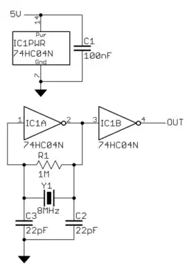
The first inverter (IC1A) is being used more like a basic inverting amplifier. R1 provides DC feedback so that the input is kept at the threshold where the output will be close to the middle. Any slight changes in the input, even noise, will be amplified onto the output. Y1 acts like a filter so that only signals at the crystal frequency are fed back into the input, which are then amplified, which then have all but their 8 MHz components removed by Y1, which are then presented back to the input but stronger this time, etc.
Normally feeding a signal directly back into the inverting input of a amplifier would null out any noise picked up. However, the crystal is cut so that it adds the right phase shift just at its intended operating frequency when the right capacitive load appears accross it. Since the two capacitors are in series from the crystal's point of view, they provide 11 pF of load by themselves. There are other inevitable stray capacitances that are significant relative to 11 pF, so the total load is more. C2 also removes some of the higher frequency components of the square wave that IC1A is trying to make, which is better for the crystal.
The output of IC1A will probably not swing fully from ground to the positive supply. The purpose of IC1B is to amplify that again to make a nice solid digital signal, which should be close to a square wave. It also isolates the load of the rest of the circuit from the output of IC1A.
In this example, there are 4 more inverters in the same package. You can use them in other ways, but make sure they are not left floating. If you need a lot of drive, for example, you could drive the remaining 4 inverters from the output of IC1B, which then gives you 4 nearly equal CMOS outputs producing the same clock signal. Tie the inputs to any unused inverters to ground.