0

I would like to better understand this topic: Minimum ON time for a buck converter

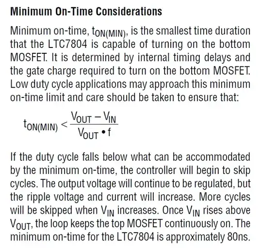
One of the answers seems to say that the minimum on-time depends on the selected MOSFET. According to the datasheet that I can find on internet, there is no information about the minimum on time. Here is an example :

enter image description here

Here is another example :

enter image description here

Does the minimum on-time depend on the MOSFET or not? It seems that it does not depend on the MOSFET, but I agree on the fact that if we took a bigger MOSFET, it will take much more time to switch ON, so it seems to have an effect on the minimum on time and on the output ripple. How can the manufacturer give minimum on-time without specifying the conditions on the MOSFET?

When we look at what is the maximum input voltage? The formula given in the datasheet does not depend on the size of the MOSFET, so it appears that the size of the MOSFET has no effect on the minimum on time. Here is an example to get Vin_max from this datasheet.

enter image description here

JRE
  • 71,321
  • 10
  • 107
  • 188
Jess
  • 2,978
  • 2
  • 24
  • 56
  • 1
    Your datasheet excerpt tells all in the first line. That is the minimum time the chip can achieve. Then you need to consider the mosfet. Both will determine the system minimum on time. – Kartman Mar 28 '24 at 08:47

2 Answers2

1

So does the minimum On time depends on the MOSFET or not

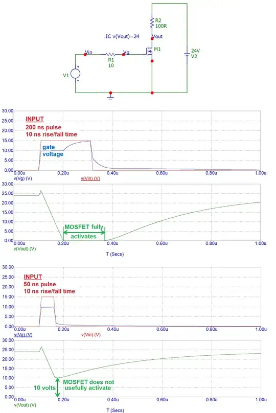
You have to make the distinction between the minimum on-time produced by the driver output and, the corresponding useful on time of the finished working circuit (a degraded version of the driver on-time). The minimum useful on-time of the finished circuit can never match the on-time from the chip due to MOSFET characteristics (for instance): -

enter image description here

In the upper plot notice that the gate voltage does not initially reach 15 volts despite the input being 15 volts. This is due to the MOSFET miller effect. The miller plateau is due to the drain voltage falling and causing negative feedback at the gate. It's very clear in the image above. Once the drain voltage has fallen to 0 volts, the gate continues to charge to 15 volts and, we can say that the MOSFET has usefully activated.

However, for the lower plot (50 ns pulse), the MOSFET cannot fully usefully activate. This of course is MOSFET dependent; I simulated an IRFZ44 but, there are MOSFETs that respond more quickly but, there will always be a degradation of the true circuit output compared to the pulse produced by the driver.

Andy aka
  • 456,226
  • 28
  • 367
  • 807
1

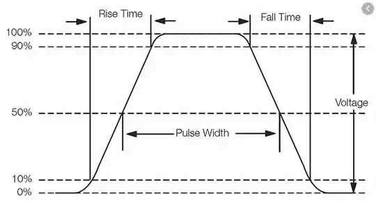
I think it's better to understand the pulse width and rise and fall times first. The following is a good representation nicked from here:

enter image description here

Apart from the minimum ON time, some chips also mention rise and fall times, but for specific capacitive loads which represent a random MOSFET's input capacitance.

This is not the case for the minimum ON time (or minimum controllable ON time) because this is limited by the gate driver itself.

The thing is, the chip generates a pulse and its duration (the dime difference between 50% of the rising and falling edges) is measured, probably right at the chip's pin but at the MOSFET's gate it can get shorter due to the trace resistance, externally put gate stopper resistance, MOSFET's internal gate resistance which comes from the manufacturing process of the MOSFET (e.g. bonding, semiconductor structure), and the MOSFET's input capacitance as all of these play a role on effective rise and fall times which determine the effective pulse width:

enter image description here

In the image above, I tried to show how the rise time can increase due to the external factors such as effective series resistance. So the effective pulse width is shorter than that at the pin.

This can't be under the chip's control. The chip guarantees a minimum on time for specific conditions (e.g. frequency, operation mode, etc) then the rest is up to the designer and the application.

Rohat Kılıç
  • 33,940
  • 3
  • 29
  • 85