Common emitter amplifiers often use resistors in their source and collector but I have been thinking, they consume power. In RF applications, would it be possible to achieve the same effect with inductors instead?
1 Answers
Yes - this is actually done somewhat often for certain classes of RF low-noise amplifiers, and manages to hit a few goals at the same time.
Part of the goal of LNA design is to produce an effective impedance match (e.g. 50 ohms) at the input, and inductive degeneration solves this rather handily. In fact, it allows you to avoid both a degeneration resistor and an impedance matching/load resistor (which would necessarily generate thermal noise at nonzero temperature).
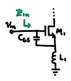
Consider the following structure (diagram is my own, adapted from the source below):
Paraphrasing from Behzad Razavi's RF Microelectronics1, here's a demonstration of how and why this works:
- Suppose an input current \$I_x\$ flows into the input pin.
- This current produces a \$v_{gs}\$ of \$\frac{I_x}{sC_{GS}}\$, and hence a current of \$I_x + \frac{g_mI_x}{sC_{GS}}\$ into the inductor.
- A voltage drop of \$sL_1\left(I_x + \frac{g_mI_x}{sC_{GS}}\right)\$ arises across the inductor
- By KVL (add the drop across the capacitor), the total voltage seen at the input port is \$I_x\left(sL_1 + \frac{g_mL_1s}{sC_{GS}} + \frac{1}{sC_{GS}}\right) \$, and hence the input impedance is
$$Z_{in} = sL_1 + \frac{g_mL_1}{C_{GS}} + \frac{1}{sC_{GS}}$$
The middle term happens to be frequency-independent and can be set to 50 ohms by tuning the inductor2. In some cases of on-chip LNAs, the supply bond wire connected to the transistor's own source provides the right range of parasitic inductance to be used directly for this task.
Some further analysis (which the book I cited explains more deeply) shows that the input impedance is roughly \$L_1\omega_T\$ (inductance * transistor's transit frequency). If the intended inductance is unachievable because the transit frequency is too high, additional capacitance can be added in parallel with C_GS.
This also has the advantage of resolving instabilities3 associated with inductive loads on the M1 drain (IIRC the instability arises due to the interaction of Cgd and the load).
Of course, the usual first-order analysis of degeneration as series feedback is still a useful lens for understanding general amplifier behavior as well - in addition to this interesting extra benefit of inductive degeneration I've outlined above.
Unfortunately, I can't speak confidently to power amplifiers.
1Prentice Hall 2011 edition, section 5.3.4 on page 284
2This disregards the bond pad capacitance, which requires an additional inductor to adequately correct.
3I haven't verified this firsthand since I don't have your simulator models or simulator, but I would speculate that this might explain the instability you're observing in this question - if it's there and happening specifically at low frequencies, rather than a sign/polarity error in the simulation or an overall instability
- 19,972
- 2
- 51
- 77
