9

As in the title, my question is basically about understanding what is the "problem" with directly-coupled (below, I will use dc for "directly-coupled" and DC for "direct current") amplifiers which necessitates the use of coupling amplifiers? Note that this question is being asked in the context of old-school discrete-circuit amplifiers, but I think that understanding that case will be helpful for me (and hopefully others) in deeply understanding the problem which differential pairs solve.

Consider for example the figure below (from Gray, Hurst, Lewis, and Meyer, 5th edition):

enter image description here

We see that the "classical" biasing arrangement for each stage (using the degeneration resistors at the emitters and voltage division at the bases) is used, and that the signal input flows through a few coupling capacitors. I should emphasize that this circuit is by no means optimal even under the discrete-circuit paradigm of the day. The point being made by the authors is around the discrete-circuit implementation using large resistors and caps whereas an integrated circuit implementation cannot (cannot use coupling caps, and so must face the direct-coupling problem head on rather than averting it by using coupling caps). I am in particular wondering about the need for the coupling caps in this question:

My question is why these coupling capacitors are necessary, and I give the two suspicions I have below. If someone is able to explain if one or the other (or something else entirely) is correct, I would greatly appreciate it. Again, I am trying to understand why we can't get away without coupling capacitors (or differential pairs).

(1) Not using coupling capacitors makes doing DC biasing hard, since then the biasing of a given stage is "connected" to an earlier stage. I am suspicious that this is the reason for the capacitors since it seems to me that, if we worked hard enough, we could overcome this by simply considering the path to the preceding transistor as being in parallel with the lower resistor in the voltage division circuit at each base and adjusting our biasing resistor values accordingly.

(2) If there is some DC component to \$v_i\$ (or some DC noise injected at any subsequent stage's input, or referenced thereto) then without the coupling capacitors we would get a dc signal which messes with the circuit. This is very hazy in my head and I can't quite figure out what "messes with" ought to mean. I guess I can argue by superposition and say that this "propagating DC signal/offset" would ride on top of whatever the intended bias voltages are, thereby changing the bias point (and also therefore the relevant small-signal quantities) and therefore the amplification at the intended frequencies?

In the end, I believe this question is related to my earlier one here which has a very nice answer from Andy, but I am still struggling to understand if the issue is about a biasing issue or a dc small signal, as per (1) and (2) above, respectively. As I write above, I suspect (2) is the issue, but I am not sure because Andy's very nice answer seems in retrospect to me to be concerned with the biasing at each stage, but perhaps I am misunderstanding.

EE18
  • 1,131
  • 10
  • 24
  • 3
    That's actually a very lousy example of a discrete-component realization of an audio amplifier. I'd probably chuck the book out the window, seeing it presented as such. – periblepsis Jan 22 '24 at 20:17
  • 1
    I am very much a novice so I have no idea about these things, but I will say in defense of this venerable text that they are probably just trying to point out some big picture points about the nature of capacitively-coupled circuits rather than actually producing a good discrete-circuit realization of an audio amp ;) @periblepsis – EE18 Jan 22 '24 at 21:10
  • Perhaps. But there's no excuse for the title used on that figure. None. It's not typical. Besides, it's essentially useless. – periblepsis Jan 22 '24 at 21:19
  • You've described your difficulty nicely. Perhaps a concrete example of a DC signal source that needs amplifying would show how EE's might tackle the problem and address disturbances. May I suggest a few different types DC signal sources: A temperature sensor (thermistor, thermocoupler, diode). Or an optical sensor like a photodiode or photoresistor. – glen_geek Jan 23 '24 at 01:17
  • The reason is (1). (2) is moot because if you are doing (1) because you are designing an AC only amp. If you try to design this kind of amp for DC then the caps are off the table and all the associated challenges are back. The bias issues are difficult enough without those caps if you're making it AC only. I think it's not actually workable for DC. We use differential pairs for DC. – DKNguyen Jan 23 '24 at 03:46
  • Thanks for your answer, it's very helpful. To be sure though, I'm not sure I follow why us being interested in AC means we don't need to worry about (2). If we didn't have those coupling caps then DC signals would penetrate (I'm trying to think of the right word given that it's DC, after all) through the system, no? And that would presumably cause bias point problems? @DKNguyen – EE18 Jan 23 '24 at 04:47
  • @EE18 Being interested in AC means you design your amplifier to remove DC so that you no longer need to worry about DC. That's the whole point of choosing to use AC-only amplifier designs. By not caring about DC it means your amplifier can do whatever you want DC-wise as long as you remove it by the time it gets to the output. – DKNguyen Jan 23 '24 at 06:20
  • If changing DC offset in the input signal disrupts your system bias, it means the DC-blocking were not chosen to be appropriately large and you no longer within the bounds of the small signal model. You are in large signal territory now. This is to be expected since real life AC amps can't be expected to have the low frequency end of the bandwidth infinitesmally approach 0Hz. – DKNguyen Jan 23 '24 at 06:21
  • 1
    I agree with @periblepsis. What is that. It's a great example of a practically useful circuit - said noone, ever. – danmcb Jan 23 '24 at 06:37

4 Answers4

6

The author's goal

The textbook illustration presents a conceptual circuit diagram of an AC amplifier. That is why it consists of simplified amplifier stages with identical biasing circuits. As the OP also noted, the goal is probably more to show the idea than the most perfect implementation. So, we should not criticize and try to improve it but use it as it is.

Basic idea

AC amplifier

Think of the coupling capacitors as "rechargeable batteries" that shift the voltage variations from the previous stage to the next stage. They do that by adding/subtracting their DC voltage in series manner to/from the voltage of the previous stage. From this point of view, biasing can be considered relative not to ground but to the previous step (i.e. each next step is "shifted" down or up relative to the previous one).

You can think of the stage outputs and inputs as DC voltage sources with different voltages. If you connect them directly, equalizing currents will flow and their DC voltages will change. The role of the charged coupling capacitors is to equalize their DC voltages. For example, if the output voltage of the previous stage is 6 V and the input voltage of the next stage is 1 V, we must connect them through a 5 V charged coupling capacitor to "fill" the difference between them.

The problem of the coupling capacitors is that at an insufficiently high frequency, their voltage will vary with that frequency; therefore these amplifiers are AC amplifiers.

DC amplifier

If we want them to be DC amplifiers, we need to connect their stages via "DC shifting elements". Such, for example, can be real voltage sources, but this is not convenient. Also, these can be resistors supplied by constant current sources; then the voltage drop across them will be constant (this trick is used by Widlar in his first op-amp). They can also be Zener diodes or "rubber Zener diodes" especially if supplied by a constant current.

Differential amplifier

Although the coupling techniques above with "hard-coupling" elements between single-ended stages are possible, they are rarely used because they transmit both the useful and undesired signals equally well. For example, if the coupling elements change their voltage even slightly, this is perceived as a useful signal and induces an offset voltage at the output. The trickier solution is to connect differential stages directly. But how is this possible?

The clever trick on which the differential amplifier is based is that (in the so-called "common mode") its "internal ground" (the common emitter point in the case of a long-tailed pair) is not fixed but "movable". So instead of the output voltage of the previous stage going down to zero voltage ground, the differential stage raises its internal ground to the level of that voltage. Then, in the "differential mode", the input voltage(s) "wiggle" around this "shifted ground".

CircuitLab experiments

Let's bring this sterile textbook circuit diagram to life with the help of CircuitLab. Due to scaling it is quite reduced; so it is good to look at it in the editor. I would like to connect more meters, but the schematic would be cluttered; so I have put only two voltmeters in the output stage to show the output voltages. They also act as a 1 kΩ emitter resistor and 10 kΩ load resistor (I have given them such internal resistances in the parameters window). The resistance values are illustrative and roughly chosen for the purpose. I propose to conduct the experiments in the following order:

Coupling capacitors

Without "messing" DC input voltage: Let's first set the AC input voltage to zero (short the input) and observe the stage output voltages and base bias voltages by hovering the mouse over the circuit diagram.

schematic

simulate this circuit – Schematic created using CircuitLab

With "messing" DC input voltage: Let's now add a small 10 mV DC component V1 to the input (the OP's suggestion) and to the outputs (V2 and V3) of the two voltage-amplifying stages. We see that the coupling capacitors decrease by that much their voltage and nothing in the circuit changes.

schematic

simulate this circuit

"Coupling" voltmeters

Before we replace the "soft" capacitors with "hard" voltage sources to make a DC amplifier, let's measure the voltages across them by replacing them with voltmeters.

schematic

simulate this circuit

Coupling batteries

Without DC input voltage: Then we adjust the "rechargeable batteries" to these voltages and put them in place of the voltmeters.

schematic

simulate this circuit

With DC input voltage: Our "direct-coupled amplifier" is ready. If we now apply the same 10 mV DC input voltage as above, the output voltages across R11 and R12 change.

schematic

simulate this circuit

Circuit fantasist
  • 16,664
  • 1
  • 19
  • 61
  • 1
    If I am understanding you correctly, you are saying that the coupling caps are solving the problem (1) I noted above? I see now that I naively said we could figure things out with respect to biasing but, in fact, if a given stage's bias point is fixed then so too is its output bias voltage which, if connected to the next stage's input, might be different than the best input bias point for that next stage. – EE18 Jan 22 '24 at 19:58
  • @EE18, Exactly! Charged capacitors allow the output and next input to be coupled in terms of AC voltage changes but at the same time separated in terms of DC (bias) voltages. – Circuit fantasist Jan 22 '24 at 20:04
  • 1
    Thank you! Just one final clarification before I accept: suppose that by some happy coincidence the biasing is not an issue. That is, it just so happens that the output bias voltage of one stage is precisely the optimal input bias voltage of the next. Thus, (1) would not be an issue in this case. Does it follow that (2) might still be an issue? That is, we would still need coupling capacitors for the reason I describe in (2)? – EE18 Jan 22 '24 at 21:08
  • @EE18, Very smart questions... I have to admit, it was a little difficult for me to imagine at first, but now (an hour after midnight) it started to appear in my mind. I think you almost got the answer. The DC component will not "mess up" the circuit but will simply add (superimpose) to the bias and AC voltage. The only difference is that if there are coupling capacitors, it will slightly change the bias voltage of the local stage; but if not, it will change gradually increasing the bias voltages of the following stages. This will move the operating points and will change small-signal gains. – Circuit fantasist Jan 22 '24 at 23:29
  • 1
    Thank you again for this very helpful discussion! I am just going to note (for myself and for posterity) that in the very nice conceptual experiments some voltages do change very slightly when we remove the caps, but this is likely because of the underlying circuit simulation (e.g. 41.67 $\mu$V in Experiment 2 on R12) and is unphysical. – EE18 Jan 28 '24 at 00:17
  • @EE18, Thanks for the response! I would be glad if nothing remains unclear. I start replying with comments here and in my answers. These 41.67 μV appear across R12 because the voltmeter VM4 is not "absolutely ideal" but has an internal resistance of 1GΩ. Together with the 10k R12, it forms a voltage divider R12/(RVM4 + R12) = 10E4/(10E9 + 10E4) = 10E-5. The other two voltmeters (figuratively named “R11” and “R12”) are "very non-ideal" because I deliberately reduced their resistance to act as "visualized resistors". I have done this trick to simplify the schematic; I hope it doesn't bother you. – Circuit fantasist Jan 28 '24 at 10:40
  • 1
    No problem, it makes total sense! – EE18 Jan 28 '24 at 20:33
4

Coupling caps are no needed if you dealing with pure DC amps. But in that case you need to ensure not stable gain only, but a very stable bias point also.

In AC amps with cap couplings the precise bias point does’t care you so much. The gain has to be held precise in both (AC and DC both).

Michal Podmanický
  • 1,695
  • 1
  • 1
  • 11
4

Well, we can only speculate why the author chose to present this as a "classical" example. Such circuits haven't been used seriously since the 1960s; or arguably 1920s, really, if transistors are replaced with vacuum tubes. But we can derive meaning from the image independently of author intent (for better or for worse, as deconstruction is wont to be :) ), so with those points in mind:

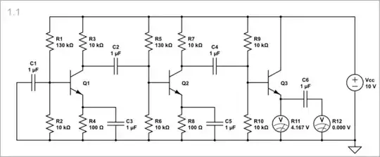
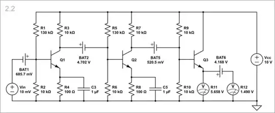
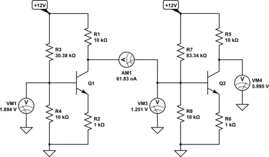
Notice the complete lack of negative feedback. There is no emitter degeneration, there is no local collector (shunt) feedback, there is no global feedback across stages. The transistors are also all same polarity.

If this is the author's intent, then it seems it could've been said more simply by saying "no feedback". Presenting it with such an example seems a bit cryptic.

And, it's more likely a better explanation applies; but to say: this is a possible reading, given the context.

The choice of dates may be more interesting. 1920s, because negative feedback in electronic amplifiers became widely available and understood academically in 1934:
Black, H.S., Stabilized Feedback Amplifiers, BSTJ 13: 1 (January 1934)
which is still an excellent article today; the properties of vacuum tubes are not so different, even in terms of biasing (BJTs and enhancement-mode MOSFETs require positive input bias, and BJTs, more current; depletion MOS and JFETs are nearly drop-in), and mainly the impedance range is lower, and gain (and especially wideband figure-of-merit) is vastly improved.

In the 1960s, transistors were new, and still quite expensive; the advantages were clear over most vacuum tubes, making them indeed economical substitutes in many circuits and devices, but only that -- substitutes, with largely similar circuitry around them, keeping transistor count low to manage bill-of-materials (BOM) cost while improving functionality and reliability.

This economic environment, combined with the hybrid (tube and transistor) circuitry, made such solutions likely, or common -- as well as transformer-coupled stages, for example a step-up transformer to adapt to a tube grid, or a step-down transformer to optimize power output into a speaker. (Transistors capable of direct speaker drive were more expensive -- power transistors were certainly around, but why use one when a small-signal transistor will do for a fractional-watt radio output?).

Complementary transistors were also few and far between. Silicon was still early in development, and germanium types were widely available -- almost always PNP, because the germanium base (literally, the base upon which the transistor is built, this is how the term arose) can be P-doped by melting indium solder on either side of it (alloy junction). For a time, upside-down schematics were a common sight -- an astute observation really, as PNPs are simply the inversion of NPNs (and needless to say, vacuum tubes are exclusively N-type, it's a lot harder to produce positron beams!) and vertically flipping the schematic and supply polarities yields the same schematic layout, signal flow from left to right, power from top to bottom, but it's electron flow from a negative source, rather than conventional current flow.

Oh yeah, electron current flow was still quite popular back then, as well. Somewhat reinforced by the success of PNP devices I suppose, but it was commonly presented in context of vacuum tubes. Probably most notably by the Navy's educational materials, which by organizational inertia, persisted much later than most (once NPNs, and indeed ICs, took over).

Anyway, complements are important because, making a DC-coupled amplifier entirely out of a single type (NPN here), is challenging, and usually requires additional supplies, and compromise in SNR, operating range (the input doesn't function near one or both supplies, or the output can't saturate very far towards them), bandwidth, cost (e.g. adding transformer coupling), etc. The success of complementary circuitry, even the very meager lateral PNPs that were offered on early (~1970s) IC processes, proved exquisitely useful, facilitating the first general-purpose operational amplifiers for example, with similar input and output voltage ranges (within 1-3V of either supply), even some fully including one supply (e.g. LM358).

So, I also think the image in question comes from a historical perspective. A vacuum tube phono amplifier for example, might use a similar circuit, but would have cathode degeneration to mitigate distortion; it wouldn't be DC-coupled because it's not required (or indeed detrimental, as phonograph pickups can have low-frequency rumble that you want to filter out -- notice coupling caps are just high-pass filter networks coupling between stages -- we can generalize their presence or effect in this way), and it's not using global feedback because that much open-loop gain, combined with that much phase shift, likely makes things more complicated, or prone to instability, and a simpler circuit will suffice. (Now, two stages cascaded, isn't a whole lot, but keep in mind, tubes have maximum gain with quite high impedances indeed -- a 12AX7 preamp might use 330k plate resistors. Even though the plate capacitance is a couple pF, this puts the HF cutoff pole not far above the audio range -- 10s of kHz. Two stages cascaded, plus feedback, means little phase margin at the upper band limit; and three is right out.)

Again, there's no reason to use such a circuit when NPN and PNP are available -- let alone when ICs are available. So it indeed seems odd to use such an example in present-day (or, really, since 1970s) context.


Ah, let me see here, what is the context of this book anyway; well, 1st edition seems rare, but 2nd starts with the opening, "In the 23 years since the publication of the first edition of this book, the field of analog integrated circuits has developed and matured", and is dated 1990, so the '60s would've been present context as of its original writing. It seems surprising that this figure would have survived into the 5th edition (you didn't mention which you're reading from, but I'm assuming the most recent, it appears widely available) to make such a point, but I suppose that's at least a possible historical route for it.


I should probably cite something for 1960s knowledge. Contemporary databooks are a good representation. I'm particularly fond of RCA's series, which are knowledgeable, practical and accessible. The RC-xx series for vacuum tubes (Receiving Tube Manual) for example are excellent, but they applied the same form to their transistor manuals too:
RCA Transistor Manual, 1964
Consider 11-7 (p.351 (353)) and onward, for example; a mix of local to multi-transistor feedback, PNP and NPN circuits, and capacitor and transformer coupling, is offered through this section. And, if you have any questions about the now-obscure transistor types, just look up, the short-form data (likely as much or more data as registered with JEDEC, to be fair..!) makes up the bulk of this book.

Tim Williams
  • 33,670
  • 2
  • 22
  • 95
  • Thank you for this absolutely fascinating answer. I'll admit that much of it goes over my head, but let me make a few comments: (1) Yes, you are correct that I'm looking at the 5th edition (I will update this) (2) As I wrote to periblepsis above, I don't think the authors' intent is to show a good discrete-circuit implementation so much as to distinguish said implementation from an integrated implementation (Fig 3.1b, if you are looking at the book). They actually note that they are not using feedback etc. in the text. – EE18 Jan 22 '24 at 23:11
  • To that end, I'm hoping to confirm if your answer (in particular the paragraph starting "Anyway...") seem to suggest that my suspicion (1) in the OP is the issue with not capacitively-coupling subsequent stage. Is that understanding correct? If so, is (2) at all a consideration? As I note in a comment in the other answer by Circuit fantasist, suppose that by some happy coincidence the biasing is not an issue. That is, it just so happens that the output bias voltage of one stage is precisely the optimal input bias voltage of the next. Thus, (1) would not be an issue in this case... – EE18 Jan 22 '24 at 23:15
  • ...Does it follow that (2) might still be an issue? That is, we would still need coupling capacitors for the reason I describe in (2)? – EE18 Jan 22 '24 at 23:15
  • Only to note that there is a (DC) emitter degeneration. – Circuit fantasist Jan 22 '24 at 23:58
  • 1
    It's a bit of everything, yes. Setting aside that some circuits should be AC coupled (at least in part, or arguably so; audio, RF, etc.), any DC in the input is DC in the output, magnified, and often that DC is a nuisance (e.g. phono), or poorly controlled. Consider the tolerance of those base divider resistors, then multiply that range by the total gain; or consider the spread in Vbe vs. temp (say 500-800mV over commercial temp range). Even a small difference, changes the operating point and therefore gain (bandwidth too) of the circuit -- and without feedback, that's no small effect. – Tim Williams Jan 23 '24 at 00:13
  • Another note, or, another angle: at this point, you may be starting to run out of meaningful textbook explanations, or, more than wrote/given reasons why they're done that way; consider breaking out the breadboard. Try it yourself! They did, back in the day; rediscover what they found out. These aren't terribly complex circuits; a half-dozen transistors can be interconnected in a fairly rich, but still tractable number of useful circuits. Of course, test-driven development is nothing without tests, so take some time to understand what underlies that: – Tim Williams Jan 23 '24 at 00:15
  • For IC manufacture for instance, there's at least variation in supply voltage, device temperature, and manufacture (junction areas, doping concentrations, resistor values, etc. vary from wafer to wafer, and between locations on a wafer for that matter), and a good circuit is immune to all of these. You might also check extremes of inputs or outputs: inputs beyond nominal range, pins reverse-biased, ESD, etc. A discrete circuit additionally has part-to-part variation, by manufacture and temperature (you don't have much choice in device matching), but that too can be dealt with. – Tim Williams Jan 23 '24 at 00:19
  • Thank you very much for all your helpful comments! Glad to know I'm not too off on understanding. Your suggestion re: actually breaking out these circuits on the bench is well taken, but I'm afraid I don't really have access to all of that :( perhaps it's time to start spending textbook money on lab kit money though! – EE18 Jan 23 '24 at 01:01
3

Here's a circuit with voltage gain of 100, implemented as two stages of gain 10:

schematic

simulate this circuit – Schematic created using CircuitLab

I've artificially introduced minor input offsets using V2 and V3. Even the slightest offset at the input is also multiplied by 100, which is why, with an explicit input of 0V, the output of this amplifier is 1V.

I assume you understood this already; that a sequence of cascaded DC coupled single-ended amplifiers will compound any input offset, until at some point one of the amplifier outputs is so far from its intended quiescent level that it is bound to clip against one or the other of its own supply potentials, as the real input signal fluctuates.

I assume that you also understand that coupling capacitors solve this issue by developing a "permanent" DC potential that bridges the potential difference between the quiescent output level on one side, and the quiescent input level on the other.

Perhaps it's not obvious that those tiny offsets can drift with time and temperature, and even if you did manage to compensate for them by some means, (perhaps you subtract 10mV at the input), that might work at 25°C, but the required offset will be very different at 40°C, or 2 years later.

Again, capacitors adjust automatically to compensate for the difference between mean DC voltages on either side. For many applications, such as audio (where frequency components below 20Hz or above 20kHz are not of interest) AC coupling with capacitors is such a simple fix that there's no real advantage to direct, DC coupled stages.

Sometimes, though, you do want DC coupled stages, because 0Hz (DC potential) is just as important to you as any fluctuations about that level.

In the discrete transistor amplifier you showed us, where capacitors lie between each stage, those capacitors charge over time to some average, DC voltage to bridge the average potential difference between the two sides. Consequently, average DC current through the coupling capacitor eventually drops to zero. If you wish to directly couple those stages, you somehow need to obtain this same condition, zero average current flowing from stage to stage. Take this single stage for instance:

schematic

simulate this circuit

It has been carefully biased to produce exactly +6.000V at the collector, but injecting even only 1μA of DC current at the input will permanently offset the output by 80mV.

Let's say we somehow manage to bias two stages so that the first produces exactly the correct quiescent potential at its output to perfectly match the quiescent potential established at the input of the second stage. In the above circuit, quiescent input potential is +1.250V. You can't just cascade two such stages directly, since connecting the 6V quiescent output of the first stage to the 1.250V quiescent input of the second would result in significant DC current being injected into stage 2's input, which would "mess up" its biasing. You have to produce a stage 1 whose quiescent output is equal to stage 2's quiescent input:

schematic

simulate this circuit

The important thing to note here is that these are direct coupled stages, and there is no direct current flowing in the path between stage 1 output and stage 2 input.

Watch what happens if I change the \$\beta\$ (current gain) of Q1 from 140 to 100, representing just one of many variations that occur between transistors of the same type, and even the same batch:

schematic

simulate this circuit

The quiescent output potential of stage 1 is necessarily different, and suddenly we have a tiny 62nA direct current flowing into stage 2's input. The consequence is a permanent 5mV offset at the output. It doesn't sound like much, but stages further along the chain will have to deal with this somehow.

That's just one change. We have temperature changing \$V_{BE}\$ and all resistance values, aging of components, dependence of quiescent levels on power supply voltage, and goodness knows how many other uncertainties. Biasing a circuit like this to maintain the same quiescent output level, under those changing conditions, is very challenging.

There are a few techniques available to mitigate these offsets in single ended amplifiers, such as negative feedback, and chopper-stabilised op-amps.

Another solution you alluded to is to employ differential amplifiers:

schematic

simulate this circuit

The two stages here are typical implementations, the first producing a differential output, the second producing a single-ended output (with respect to ground). You could cascade as many of the first type as you desire.

V2 introduces an undesired +100mV offset to both input potentials, but the nature of a differential amplifier is to remove that offset, by performing the subtraction \$V_{IN1} - V_{IN2}\$.

You still have op-amp imperfections to worry about, which will cause OA1 and OA2 to introduce introduce slight offsets of their own, but if those two devices are well matched, and have the same temperature and age similarly, those offsets will be similar, and the following differential stage can all but cancel them. This assumption is little a naive, there will be other things to cause an offset at OUT, but the worries are far fewer than for direct coupled single-ended amplifiers.

Simon Fitch
  • 34,939
  • 2
  • 17
  • 105
  • This answer was absolutely beautiful, thank you so much for taking the time to type it out. I've gone ahead with the other answer as it was first and equally helpful, but if it's OK I'd greatly appreciate it if you could expand on the differential circuit argument you gave at the end as I got lost there. In particular, as I followed your discussion of single-ended direct-coupled circuits, it seemed to me that the problem we found via your experiments was that any mismatch etc. would result in current flowing between stages. In the differential circuit case you remark that the differencing – EE18 Jan 28 '24 at 00:26
  • action ensures that any spurious common mode voltage will be (ideally) rejected (by that differencing). But isn't this something different? That is, in my head I'm not seeing how the direct coupling problem (which I thought was quiescent current between stages) is solved by differential circuits. – EE18 Jan 28 '24 at 00:27
  • @EE18 We always have input and output resistance to consider, through which current will cause a voltage shift, or a voltage shift will cause current, and so really current and voltage are just different descriptions of the same thing. Differential amplifiers still suffer from that issue, but they have a symmetry absent in single ended ones... – Simon Fitch Jan 28 '24 at 02:43
  • @EE18 Provided that symmetry (component matching) is good, current/voltage offsets present at the inputs and outputs of a differential stage are equal on either side of the line of symmetry. Input bias currents are equal, input and output resistances are equal, and so on. Any offsets introduced as a result of these may therefore be considered part of the common mode signal, which is subject to a far lower gain. – Simon Fitch Jan 28 '24 at 02:49