Basic idea
Single-ended configuration
In direct-coupled amplifier stages, the output voltage of the previous stage is a sum of the amplified AC voltage and the quiescent DC voltage. This composite AC+DC output voltage should be “shifted down” almost to ground level so that the input voltage of the next stage “wiggles” around the zero level. This actually means that a DC voltage equal to the quiescent DC voltage must be subtracted from the composite AC+DC output voltage so that only the AC voltage remains.
Also, under the influence of temperature, the quiescent output voltage and the shifting voltage slightly vary. To be compensated, these changes must be equal and opposite. But in this “single-ended configuration” the two voltages are not under the same conditions - the output voltage is referenced to ground and the shifting voltage is floating; this makes compensation difficult.
Differential configuration
In contrast to the single-ended configuration, here, to make perfect compensation, the two DC voltages are exactly the same and both referenced to ground. However, the resulting AC voltage is "floating" and requires a differential input to the next stage. Note that the “shifting" DC voltage is introduced by another input voltage source which determines the behavior of the former.
Figuratively speaking, in common mode the differential stage “lifts" its internal ground (the common emitter point) to the level of the two output voltages of the previous stage, and in differential mode, these voltages "wiggle" around this "shifted ground". So, the clever trick on which the differential amplifier is based is that in common mode its "internal ground" is not fixed but "movable", following.
Conceptual circuits
We can illustrate the ideas above using simple equivalent electrical circuits.
Immovable real ground
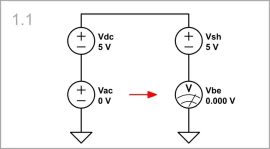
Let's first consider cascading two single-ended stages. The output of the previous stage is represented as two voltage sources (5 V quiescent voltage Vdc and input voltage Vac), connected in series. The "shifting" voltage source Vsh is connected oppositely and in series to Vdc so that its voltage is subtracted. The resulting voltage appears across the voltmeter Vbe (its voltage is decreased to 1 kΩ to roughly resemble a base-emitter junction).
Vac = 0: In the initial case, Vsh compensates Vdc, and the Vac zero voltage appears across Vbe.
simulate this circuit – Schematic created using CircuitLab
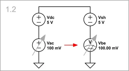
Vac = 100 mV: When Vac slightly increases above Vdc...
simulate this circuit
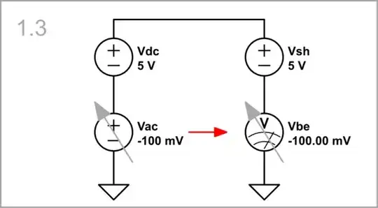
Vac = -100 mV: ... or decreases below Vdc...
simulate this circuit
... its variations appear shifted down across Vbe (Vac "wiggles" around ground).
The disadvantage of this single-ended DC coupling is that the Vdc and Vsh variations act as an input signal and are amplified by the next stage (try it by slightly changing Vdc and Vsh, and looking at Vbe). Let's see how we can solve this problem.
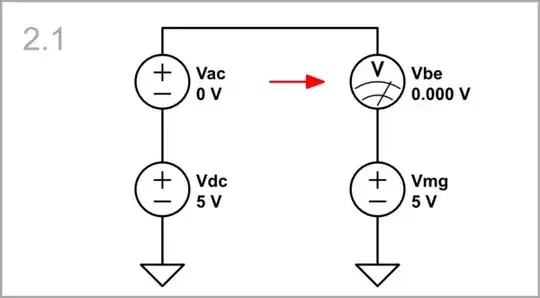
Immovable virtual ground
With the same success we can put Vsh below Vbe instead above (i.e. to attach it to the next stage). It actually means to "lift" the ground with Vdc.
Vac = 0, Vmg = 5 V: If we keep the movable ground constant (Vmg = Vdc = 5 V)...
simulate this circuit
Vac = 100 mV, Vmg = 5 V: ... and increase Vac...
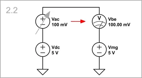
simulate this circuit
Vac = -100 mV, Vmg = 5 V: ... or decrease Vac...
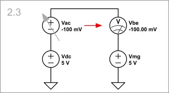
simulate this circuit
... the result is the same - the Vac variations appear across Vbe. This mode corresponds to the differential mode of the differential amplifier.
Movable virtual ground
But if we move the ground in the same direction...
Vac = 100 mV, Vmg = 5.1 V: ... simultaneously increasing both Vac and Vmg...
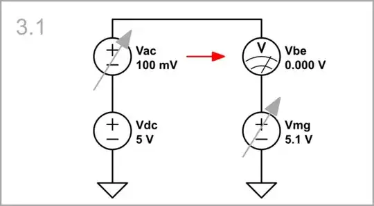
simulate this circuit
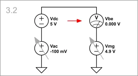
Vac = -100 mV, Vmg = 4.9 V: ... or decreasing them...
simulate this circuit
... the result is the same - Vbe = 0 V. This mode corresponds to the common mode of the differential amplifier.
But what is the advantage of this way of coupling amplifier stages? To answer this question, let's see how the "movable ground" is implemented in differential amplifiers.
Movable ground implementation
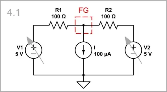
This "long-tailed pair" arrangement consists of three "sources" in parallel - two (input) voltage sources V1 and V2, and a current source I. For our purposes, we can ignore the current source and focus only on the two voltage sources. So this differential configuration is doubled compared to the single-ended configuration above.
Movable ground: If the two input voltages change in the same way (common mode), the midpoint FG will also change this way, and will act as a "following movable ground".
simulate this circuit
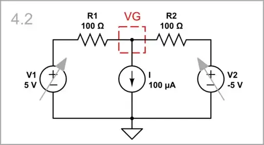
Fixed ground: If the two input voltages change in the opposite directions (differential mode), the VG midpoint voltage will not change, and will act as a "virtual ground".
simulate this circuit
So the mechanism of this differential coupling is as follows: When V1 = V2, the "movable virtual ground" moves freely to the Vdc level, and when V1 = -V2, it is fixed there. Its advantage is that the "movable ground" is automatically set equal to the input DC voltage and will move when it varies due to temperature for example.
Practical circuit
This concept can be seen in the practical circuit of the transistor differential amplifier below. The previous stage is simplified and split into two halves, and they are placed on either side of the next step.
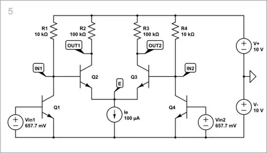
simulate this circuit
You can conduct the conceptual experiments above by this practical circuit.
Conclusion
DC amplifiers are made by cascading differential amplifier stages because their input voltages are referenced to a movable internal ground which follows the input quiescent voltages.
