3

I am trying to build a full adder with NAND gates. I have a transistor implementation:

Full adder circuit

I am getting the wrong output voltages for Cout and S; is there a way to fix this? Is it my resistors that have incorrect values? I am pretty sure the circuit is well connected; it is more a problem of resistors. What can I do to fix it?

JRE
  • 71,321
  • 10
  • 107
  • 188
Jake
  • 113
  • 4
  • 2
    You need to actually *design* them if you want to chain them. See here for one such approach. – periblepsis Jan 11 '24 at 14:41
  • @periblepsis I'd say this can be done simply enough with intuition and trial and error, no need for calculations. However you do need the intuition, and two minutes playing with this circuit in a simulator like falstad/circuitjs would highlight wherever the problem is.. – user253751 Jan 12 '24 at 00:15
  • @Jake how did you decide the resistor values? – user253751 Jan 12 '24 at 00:15

3 Answers3

4

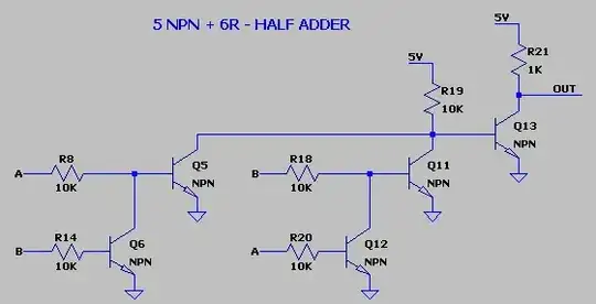
First of all, some of your resistor values need adjusting.

R16, R24, R25 need to be higher (like 10K).

Q6 needs a resistor on its base (like 10K).

Generally speaking, all collector and base resistors can be higher (like 10K) except the ones at the output (R20 and R23), which would be lower (like 1K).

If the output of any NAND stage drives only one base, then you can omit the base resistor.

R9, R10, R21, R22 are not needed.

If you fix the resistor values, your half adder design for A/B with output at R8 is basically correct in that it implements the half adder truth table. Let A, B be int input and H be the half adder result at R8 then...

A B    H
0 0 => 0
0 1 => 1
1 0 => 1
1 1 => 0

The carry logic is not correct. Your current design produces...

H Cin    Cout
0 0   => 1 (should be 1 for A=B=1, but should be 0 for A=B=0)
0 1   => 0 (should be 1 for A=B=1, but should be 0 for A=B=0)
1 0   => 1 (not correct)
1 1   => 1 (correct)

The problem is that the carry logic in your design only depends on the half adder result and the input carry. For cases (A=1 and B=1) H is 0, so it gives incorrect results for those cases.

The truth table for a full adder should look like

A B Cin    S Cout
0 0 0   => 0 0
0 0 1   => 1 0
0 1 0   => 1 0
0 1 1   => 0 1
1 0 0   => 1 0
1 0 1   => 0 1
1 1 0   => 0 1
1 1 1   => 1 1

Designing this out of NAND gates is of course not the most efficient design. Here are some examples that use less transistors/resistors.

enter image description here

enter image description here

user4574
  • 12,214
  • 18
  • 33
  • 1
    The three-transistor half adder doesn't work as shown. There are two problems: input sections need mutual isolation, so either a diode between each input section and Q3's base, or a Q4 in parallel with Q3, and one input section driving Q3 base, another driving Q4 base. That makes the logic work. The output still needs some form of voltage regeneration, like two inverters in series and a buffer, etc. – Kuba hasn't forgotten Monica Jan 12 '24 at 01:02
  • @Kubahasn'tforgottenMonica I agree. I was in a rush, and I forgot to put in resistors on the base of Q1 and Q2. The main point was that the design can be done with far fewer transistors. I will edit this. – user4574 Jan 13 '24 at 04:34
  • Half-adders have two outputs, your circuits have only one each. – Stig Hemmer Jan 15 '24 at 09:41
4

Rather than point out the issues in the original (like inconsistent / missing resistors and misconnected carry-out logic), here's a working example with those problems fixed (simulate it here):

enter image description here

All-NAND Logic design follows this example: https://www.eeweb.com/full-adder-nand-equivalent/

Key point to note in your design: mind the bias of each NAND's transistor input. In the NAND gate, the 'upper' base the pair will need a higher voltage than the 'lower' one because the upper one has the lower one’s Vce voltage added to it. Using separate base resistors for each input papers over this issue.

This isn't as much of a problem if you use transistor-based NOR. Unlike the NAND, the NOR gate has both emitters grounded, and so each transistor turns on at the same bias voltage.

Speaking of which, here's what an all-NOR version of a full adder looks like (simulate it here):

enter image description here

Looks the same, doesn't it? Indeed, in this case just substituting NOR for NAND everywhere yields the same result. All the transistors have grounded emitters; making it easy to merge and delete some of the base resistors if that is a design goal. (In fact you only need three: one each for A, B and C-in inputs.)


Implementing full adders out of NAND is aesthetically pleasing. It has those nice symmetric XOR (half-adder) structures that are things of beauty. Now, is it the most efficient way to make an XOR, let alone a full adder? Nope.

Anyway, extending on this all-NAND idea, some argue that NAND is the 'universal gate' since you can make any logic out of it. Well, no; you can do that with NOR as well.

Related: What is the lowest level of CPU programming above transistors?

In fact, the best known example a computer made from just one 'universal' gate type is the one that flew to the Moon: the Apollo Guidance Computer. That beast used just one kind of logic IC, a dual 3-input RTL NOR.

On the other hand, I've not heard of anything nearly as significant as the AGC being built entirely of NAND gates. Have you?

hacktastical
  • 53,912
  • 2
  • 49
  • 152
3

Be consistent with your base resistors. Use 10k for every base and 1k for every collector pull-up. Otherwise, the base-emitter junctions are going to mess with the output voltages (by shorting them to ground).

And don't omit base resistors (they're missing for Q5 and Q6).

Jonathan S.
  • 18,288
  • 34
  • 56