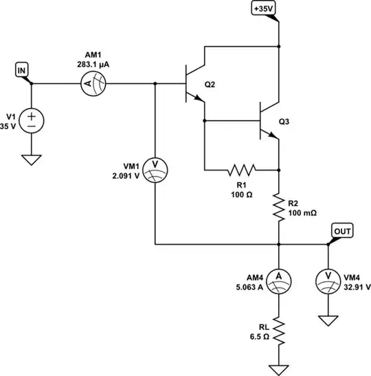
With \$\beta=20,000\$, and output transistor collector currents up to 5A, you are expecting base current to never exceed \$\frac{5A}{20000} = 250\mu A\$, which must be sunk/sourced by your yellow transistor.
I don't think there's a transistor in existence that can't handle that tiny current, or even 100 times that. Given that yellow's \$V_{CE}\$ will be only 4V or so, even passing tens of milliamps it would only dissipate tens of milliwatts, so you could use pretty much any signal transistor in this role.
It's hard to explain with no component labels, so I'll draw a simplified equivalent here:
simulate this circuit – Schematic created using CircuitLab
This is just the upper half of the push-pull pair, with a load that draws about 5A at maximum voltage.
I think your 4.7Ω resistors are not useful. Did you misplace resistor R1? R1's role here is to provide a discharge path for Q3's stored base charge, so it can switch off quicker.
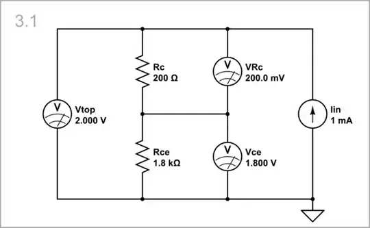
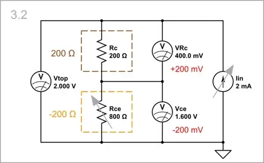
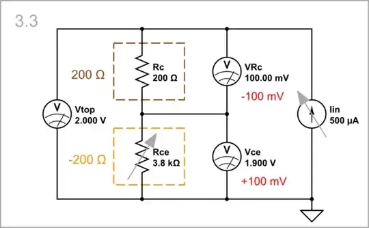
As output current (shown by ammeter AM4) rises, Q2's base current (ammeter AM1) does too, always a factor of about 20000 lower. To be safe, let's assume base current at maximum load won't exceed 300μA.
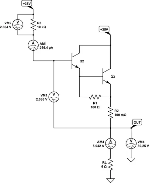
All of that current must be sourced from whatever is driving the base of Q2. If you are not driving IN directly from some voltage source, as is your case when using the VBE multiplier, that base current can only come via the top-left resistor in your schematic. that's R3 here:
simulate this circuit
As you can see, base current is causing R3 to develop a significant voltage, 2.7V shown on VM2. This limits the maximum possible base potential to be significantly lower than the 35V supply, and consequently maximum output voltage is reduced by that amount too. Therefore, before you begin considering the resistances for your VBE multiplier, you must first establish a reasonable value for R3.
You must consider that the voltage across R3 can rise to 70V, as input (Q2 base) potential is pulled down towards -35V. Even though Q2's base current will never exceed 300μA or so, R3 current will be significantly more than this.
On top of that, you will require significantly more than 300μA through R3 (with Q2 base potential at maximum), because you must have current "left over" to bias your VBE multiplier.
With this design you are forced to have huge variation in current through R3, as the input swings between +35V and -35V, and this will affect the VBE multiplier's own voltage drop. To keep the voltage across the VBE multiplier reasonably constant, at about 4V, you want to keep that current swing to a minimum.
Your choice of R3 is at least as important as your choice of resistances for the VBE multiplier, so let's examine how you might choose R3. I'd start with a guess as to what a reasonable bias current for the VBE multiplier would be, add that to base current, and see what value for R3 emerges.
Since you require 30V maximum at the output, you require \$30V + 2V_{BE} \approx 32V\$ at Q2's base, meaning that R3 cannot ever be permitted to drop more than \$35V - 32V = 3V\$ when the input is near maximum.
Q2 base current and VBE multiplier current is all sourced via R3 (from the +35V supply rail), and must not cause R3 to develop more than 3V. Assuming that the VBE multiplier requires 1mA, then total current through R3 will be \$1mA + 300\mu A = 1.3mA\$, and R3 must be at most:
$$ R_3 = \frac{3V}{1.3mA} \approx 2.2k\Omega $$
When the input is -35V, the potential at Q2's base is pulled down to around -31V (accounting for the VBE multiplier's voltage of 4V or so), and the voltage across R3 rises to \$(+35V) - (-31V) = 66V\$.
With 66V across R3, current in R3 will be:
$$ I_{R3} = \frac{66V}{2.2k\Omega} = 30mA $$
Power in that resistor, with 66V across it, would be:
$$ P_{R3} = \frac{V^2}{R_3} = \frac {(66V)^2}{2.2k\Omega} = 2W $$
R3 will have to be quite beefy, but it only spends very little time during an input cycle (when the input is near -35V) dissipating 2W, so probably a smaller device would be fine.
This means that the current drawn through the VBE multiplier will vary between 1mA and 30mA! Let's hope that the VBE multiplier voltage will remain close to 4V throughout this large variation in current. It won't, but there is hope:
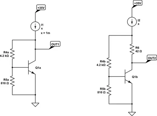
simulate this circuit
Here I've calculated R4 and R5 as follows. First, when current is at a minimum of 1mA, I want Q1 to be passing at least 20% of that (as a rough starting figure), and as current increases the transistor passes an ever greater fraction. I also want 4V across this VBE multiplier, enough to bias all output transistors slightly "on".
R4 and R5 form a potential divider, and their junction will have potential \$V_{BE} = 0.65V\$:
$$ 4V \times \frac{R_5}{R_4+R_5} = 0.65V $$
At a guess, current through R4 and R5 should be roughly 80% of the minimum bias current of 1mA (that's 800μA), leaving 20% (200μA) for the transistor:
$$ R_4 + R_5 = \frac{4V}{0.8 \times 1mA} = 5k\Omega $$
Solving those two simultaneous equations gives me:
$$ R_4 \approx 810\Omega $$
$$ R_5 \approx 4200\Omega $$
This is what happens when I sweep current (x on the horizontal axis) between 0 and 30mA. The blue trace below is OUT1 from the circuit above left, and orange is OUT2 on the right:

The classic VBE multiplier doesn't work very well, but behaviour can be improved by adding R6. The value of R6 is calculated as the slope of the blue trace in the straight region, inside the green markers. This slope is the ratio change in voltage divided by change in current:
$$ \frac{\Delta V}{\Delta I} = \frac{880mV}{21mA} = 42\Omega $$
That's the dynamic resistance of the VBE multiplier, causing it to add a certain voltage per ampere of current, rather than staying fixed. By inserting a resistor R6 of this same value, we effectively subtract the same voltage per ampere of current, that the entire VBE multiplier adds, which flattens out the curve.
You should try your circuit with all these resistor values in a simulator, under various load and input conditions. You'll no doubt need to tweak things a bit, but at least you have an idea of how I would approach the problem.
I don't think the design is a good one; you could achieve much better results using a constant current source instead of R3. Take a look at my answer about the diamond buffer to see a current source used in this very scenario.


https://electronics.stackexchange.com/questions/449914/vbe-multiplier-with-emitter-resistance-cancellation/449975#449975
– Fabio Barone Jan 05 '24 at 01:21