1

Design an audio amplifier that takes input from a small microphone and can drive a small speaker. A condenser microphone can be used. The audio amplifier must be based on discrete devices and audio transformers may be used if needed. However, op-amp or IC amplifiers CANNOT be used. Moreover, base your design on locally available MOSFETs and BJTs. Justify the selection of transistors for each specific stage. Design Specifications:

  1. AC output power = 2 Watt (8 Ω Speaker) (Ground Referenced preferably)
  2. The amplifier's frequency response should be 100 Hz to 20kHz or above at 3 dB level.
  3. The audio amplifier should qualify for the given experimental testing standard. DC Power Supply: ±12 V (dual power supplies only allowed in the last stage of the pre-amplifier stage) Overall Amplifier Gain: 1000 V/V (60 dB) Pre-Amplifier Specifications: • Zi > 100kΩ if BJTs and 1MΩ if MOSFETs, Zo ≥ 5kΩ Power Stage:(Only Class AB Stage) • RL = 8Ω • Vo = 5 Vrms

This is the Oscilloscope View of the output signals. There are 3 BJT Pre-Amp Stage and Class AB with Driver Stage Power Stage. The red signal is output after 1st transistor, Blue after 2nd, Green after 3rd and Yellow at the Output.

Image 1 Description: This is the Oscilloscope View of the output signals. There are 3 BJT Pre-Amp Stage and Class AB with Driver Stage Power Stage. The red signal is output after 1st transistor, Blue after 2nd, Green after 3rd and Yellow at the Output.Do note that this is the oscilloscope view for a 1k sine wave input with 5mV amplitude or 4mV RMS.

This is the Frequency Response of the Circuit. 20dB Gain after the first transistor, 40dB after 2nd and 60dB after 3rd. The Pink line is the gain at the output.

Image 2 Description: This is the Frequency Response of the Circuit. 20dB Gain after the first transistor, 40dB after 2nd and 60dB after 3rd. The Pink line is the gain at the output.

This is the pre-amp stage. The first two BJTs are biased based on the 1/3 Vcc rule. These are connected with only a +12V power supply. Meanwhile, the last transistor is biased so that it allows a +6V and -6V signal swing. It has +12V power supplies attached to all stages and a -12V power supply only attached to the final stage of the pre-amplifier stage. The capacitors have been set so that the Fl is set at 100Hz.

Image 3 Description: This is the pre-amp stage. The first two BJTs are biased based on the 1/3 Vcc rule. These are connected with only a +12V power supply. Meanwhile, the last transistor is biased so that it allows a +6V and -6V signal swing. It has +12V power supplies attached to all stages and a -12V power supply only attached to the final stage of the pre-amplifier stage. The capacitors have been set so that the Fl is set at 100Hz. I have tried to achieve impedance-matching of the Rout of one stage with the Rin of the next. The coupling capacitors have resistors in series so that the biasing remains intact but the gain can easily be modified.

Class AB Stage

Image 4 Description: This is the Class AB with input going in after passing through 20uF capacitors. There are 15k resistors for the biasing of the BJTs. There are two TIP22(NPN) at the top connected in Darlington form and two TIP127(PNP) connected one after the other in Darlington form. The biasing has been done by 6 diodes. A 5 ohm feedback resistor is attached between the power stage input and output.

Question: I want to know why when I send a signal of 1kHz or less, the sound is clear but as soon as the frequency goes higher the sound becomes like pulses or it starts sort of motorboating. This is apparent when I just play sine waves on a speaker. And when I play a song, some low-frequency sections play okay but others are motorboating/distorted. I have tried decoupling capacitors etc but that just makes it worse. I would need a complete explanation and calculations of any changes involved or for any new values of resistors and capacitors.

  • 3
    This looks like a homework assignments, so we will expect you to show us that you have made a substantial effort to do the work yourself. Show us what you have so far and then ask a specific question. – Elliot Alderson Dec 29 '23 at 19:34
  • You might want to google "power amplifier classes" and start learning about the different types of power amplifiers before proceeding with your project. The question doesn't specify a particular class. And that decision has to be made before beginning to design any specific power amplifier circuit. – scorpdaddy Dec 29 '23 at 19:39
  • What does the input impedance specification for the pre-amplifier, $Z_i\gt 1:\text{M}\Omega$, tell you about the semiconductor device family to use? Both in general as well as when considering noise? And what do you calculate as the input impedance for your existing pre-amplifier design? – periblepsis Dec 30 '23 at 02:10
  • I have made the input impedance about 160k. Which is something I asked the professor that it would be suitable if we use a BJT input stage. – Azlaan Ranjha Dec 30 '23 at 08:26
  • @AzlaanRanjha No. What I see in the schematic is not 160k input impedance. Where do you get that number? And for high impedance, you would want to design the first stage using a JFET device. (Perhaps in combination with a BJT.) Examine JFET input opamp block diagrams/schematics. For example, the OPA827 might be a start. Another would be here. Are you stuck using BJTs only? – periblepsis Dec 30 '23 at 22:06
  • 1
    @AzlaanRanjha There's a nice design from Elliot Audio using BJTs that can be arranged to have high input impedance and an output that is 1000 times lower in impedance while providing a gain of 10. It may be noisier than a JFET input 1st stage. But that's not in your specifications. So BJTs can be put in service. But the 1st stage should not be your basic (educational-only) CE topology. That's going to make things tougher. – periblepsis Dec 30 '23 at 23:10
  • @AzlaanRanjha You appear to have two separate specifications. One for the pre-amplifier (which for reasons I can't fathom says that its output impedance needs to be at least 5k.) One for the output stage, which appears to conflict with another spec that says 2 W into 8 Ohms. The spec for the output stage says 5 Vrms into 8 Ohm. But that's over 3 W. Not 2 W. So that's a bit of a conflict in the specs, as I skim over them. Some clarifications are needed, I think. – periblepsis Dec 30 '23 at 23:21
  • @AzlaanRanjha One more clarification is needed, I think. Does the speaker have to be ground-referenced? Or can it be bootstrapped (tied to either the (-) or (+) rail?) If there are no restrictions about that, then other options open up. Also, it looks like you are using only one side of your available $\pm12:\text{V}$ supply. Is there a reason for that?? – periblepsis Dec 31 '23 at 10:27
  • @periblepsis I have tried this circuit but to no avail. Currently, I have made a few changes to the circuit and would be happy to share the images of those. The circuit works well for frequencies of 1k or less but as soon as I go over 1k it starts motorboating. Additionally, we are only allowed dual power supplies in the last stage of the pre-amplifier stage. Nowhere else. – Azlaan Ranjha Dec 31 '23 at 10:59
  • @AzlaanRanjha You missed out specifying that detail -- about only using +/- 12 for the output stage. That's a serious failure in writing out your question! I can easily adjust the schematic I provided below to accommodate that. But you really need to write more when you write out a question. I will wait for a more thorough set of specs from you before writing further. – periblepsis Dec 31 '23 at 11:02
  • Let me rewrite the question. With the changes I have made in the circuit. It would help clear things out much better hopefully. If u just give me 5 mins. Additionally, I want to thank you for you help. It really means a lot. – Azlaan Ranjha Dec 31 '23 at 11:03
  • @AzlaanRanjha I'll +1 your question once I see better details. – periblepsis Dec 31 '23 at 11:05
  • @periblepsis I have made the edits with all the details. Let me know if you want to know anything else. – Azlaan Ranjha Dec 31 '23 at 11:20
  • At a closer look, that power stage is bonkers. The 5-Ohm "feedback" resistor serves no other purpose apart from screwing things up. This is a positive feedback resistor, in an amp stage that has a voltage amplification somewhat less than 1. Feedback resistors make sense in negative feedback, as a way to limit overall gain of the circuit. Here, it merely loads your signal source (the preamp?) excessively, if the source has some kOhm output impedance. I believe the power totem transistors hardly even open, in response to the AC input you provide. Remove that resistor. – frr Dec 31 '23 at 21:58
  • Also, if those passive AC-coupling capacitors are the substance of your "driver stage" for the output transistors, that solution is sub-prime for several reasons. It won't drive the power transistors properly (enough), the capacitors will discharge / settle on a DC offset. You need an active driver stage, see my answer for details / inspiration. In a class AB amp, without significant excess open-loop gain, and a tight negative feedback, you'll also get quite some crossover distortion - unless you bias the output totem into a fairly hefty quiescent current, close to class A. – frr Dec 31 '23 at 22:09

2 Answers2

4

your questions

Why is the signal having an offset and improper signal swing after the preamp stage

I think you mean the green curve and that this trace was taken at a point just after the series output capacitor and before your power amplifier stage. If so, then the reason it is biased with a DC offset is because of \$R_{16}\$, \$R_{17}\$, and \$R_{18}\$ in your power amplifier stage image. That resistor divider does work out pretty close to your DC bias in the green trace.

and why is the signal so distorted at the output?

There's an RC time constant operating here on one side of the cycle (no active device doing anything) and an active device working the other side. It's hard to know anything more, because we don't know if the output is diminished (attenuated) so the exact RC timing is obscured from us.

My guess would be your \$R_{26}\$, \$R_{27}\$, and \$C_{11}\$ are the cause. This could cause one half of your 2-quadrant drive to go inactive and that would explain the RC timing.

It would be easy to test. Just change \$C_{11}\$ by a factor of 10, either way.

What seems to be the issue if I biased the class AB at 20mA and have resistances of 565 ohms and 0.7V biasing of TIP31 and TIP32?

I'm not sure what this means. I almost think I do, then I find I know I don't. So I'd need more explanation from you.

a thought about the pre-amplifier stage

For very high input impedance with BJTs (I prefer JFETs here... but just saying), I really do like what Elliot presents in Figure 4 here. It's a beautiful design. I like it still more when I see it each time, again.

Let's set it up to meet the indicated high impedance:

schematic

simulate this circuit – Schematic created using CircuitLab

The above schematic does meet the input impedance requirement that you were given. \$I_{_{\text{C}_\text{Q}}}\approx 200\:\mu\text{A}\$ and the output impedance of this circuit is \$\approx 1.1\:\text{k}\Omega\$. (If you really need \$5\:\text{k}\Omega\$ then just add a \$3.9\:\text{k}\Omega\$ series resistor to the output.)

This gets halfway there: \$30\:\text{dB}\$. The rest can be done in a simple class-A or class-AB amplifier stage. This breaks up the circuit into two explainable parts: a pre-amplifier with gain (as above) and a power amplifier with gain (unshown.) Half of the total gain performed with one, half with the other.

Here's the output using LTspice:

enter image description here

I'm using a \$6\:\text{mV}\$ peak input signal as this is about what your input should be given the \$60\:\text{dB}\$ gain specification and the output power into \$8\:\Omega\$.

The output above includes overlapped outputs over the temperature range from \$-20^\circ\:\text{C}\$ to \$+45^\circ\:\text{C}\$ and using BJTs that vary in \$\beta\$ by a factor of \$2.5\times\$. It just works. No cutoff occurs.

I did add a \$10\:\text{M}\Omega\$ resistor load at the output so that the capacitor there wasn't floating. But that's all. So it's the circuit as presented above.

Here's a simulation that uses a very cheap electret microphone:

enter image description here

That is using a typical and cheap low sensitivity electret together with an ambient SPL of about 60 (a normal conversational level of audio.)

By the way, I said I really like Elliot's design.

complete design

You've said that you don't want the speaker to be bootstrapped. So I'll toss out that idea. (The benefit is that I can use one resistor instead of using a current source structure. But that's your call here.)

You've added that you must use a class-AB. So I'll go with that, as well.

I've already provided what I consider to be a very good voltage amplifier topology, above. It will work using varying supply voltages (constrained by their choice, but without failing to continue operating reasonably well, regardless.) It performs the same over widely varying temperatures of operation. It performs the same over widely varying transistor parameters. It's just... good.

So why not re-use it as far as possible?

Because there is so much voltage overhead to work with, I'm going to go with Sziklai pairs for the class-AB power quadrants and I'll use the usual \$V_{_\text{BE}}\$-multiplier to maintain their voltage separation.

But my goal here is to illustrate re-use of good design sections.

Let's look at a Elliot's design but this time as a block diagram:

schematic

simulate this circuit

All I did was to hook up the NFB input of the left section with the NFB output of the right gain-setting section and then tie ISRC, FB, and OUT together. And that was it.

But these are still useful individual blocks and they can be used with the class-AB stage without change!!! (Except, possibly, adjustments for the reference voltage and/or current source magnitude and associated small details. The block concepts remain.) These simple building block concepts are just as useful there as they were in the pre-amplifier. So this is exactly what I'm going to do.

Here's what the resulting block diagram will look like:

schematic

simulate this circuit

Note the re-use of good tools. We only need to add the creation of a \$V_{_\text{BE}}\$-mulitplier and two quadrants of class-AB drive for the speaker. The rest was just replication of what has already worked so well.

Let me fold things together a bit:

schematic

simulate this circuit

It's still the same block diagram. And the voltage rails can be changed to, say, \$\pm 8\:\text{V}\$ and the output will be just as before. Same gain, nearly the same THD, etc. It handles power supply ripple with ease. And you can change out various BJTs with varying key parameters on \$\beta\$ and \$I_{_\text{SAT}}\$ and it still works just as before. It is elegant.

Here's the final schematic:

enter image description here

Here's the bode plot:

enter image description here

(Note: I reduced the pre-amplifier input capacitor by a factor of 1000, to about \$10\:\text{nF}\$, to dampen the gain at very low frequencies and produce the above bode plot.)

At \$1\:\text{kHz}\$ the gain is:

enter image description here

So for the \$-3.0103\:\text{dB}\$ points we are looking for \$57.33\:\text{dB}\$.

I've circled these approximate \$-3.0103\:\text{dB}\$ points. So you can see the bandwidth. This betters your specification on the high frequency end. You didn't provide one for the low frequency side. But you can see what it is here. Roughly speaking, from \$50\:\text{Hz}\$ to \$22\:\text{kHz}\$.

And here's the input and output signals for a \$1\:\text{kHz}\$ input signal:

enter image description here

A nice gain of about 1000.

Beauty and functionality!

One remaining detail. Apparently there's still that \$5\:\text{k}\Omega\$ pre-amplifier stage output impedance specification. To solve this (if you need to) then stick a \$3.9\:\text{k}\Omega\$ resistor in series with \$C_4\$ in the full schematic I provided above and call the first stage the pre-amplifier and the 2nd stage and class-AB 2-quadrant drive as the power output stage. That breaks it up into two parts and satisfies all requirements. Leave a jumper there so you can just replace the jumper with the \$3.9\:\text{k}\Omega\$ resistor when and if the teacher complains. That should shut them up, then. And it won't change the output even the tiniest bit.

Unless an error is found, this is my final contribution to your question. I'm done.

(The above doesn't depend in it, but for a good process to follow in designing thermally stable current sources using the specific structure used above, see here).

periblepsis
  • 8,575
  • 1
  • 4
  • 18
  • The output signal is cutoff using this circuit – Azlaan Ranjha Dec 31 '23 at 12:30
  • @AzlaanRanjha If you mean the circuit I proposed, it's fine. I'll add the output. – periblepsis Dec 31 '23 at 16:06
  • @AzlaanRanjha Please have a look. Over a wide temperature range and varying BJT behavior it works reasonably well and the voltage gain holds quite tightly at about 30.6 plus or minus 0.1 over temperature and BJT variation. – periblepsis Dec 31 '23 at 16:12
  • Hmmm...still I have doubts about the audio output. Have you seen the changed circuit I have given above after the edit? – Azlaan Ranjha Dec 31 '23 at 18:49
  • @AzlaanRanjha No. I've not. But I'm telling you to avoid certain structures. I've very little interest in helping you struggle over ideas that are inappropriate and have no chance, with the only outcome being, hopefully, that I someday convince you. My goal isn't to spend time proving why things won't work. – periblepsis Dec 31 '23 at 18:55
  • @AzlaanRanjha Nor is my goal to examine one hack after another, with no end in sight, explaining why each has problems. And there is still the power stage to deal with. Can it be class-A? – periblepsis Dec 31 '23 at 19:04
  • The power stage has to be a Class AB. The changes that I have made work well and the only issue that there seems to be is that at any frequency higher than 1kHz there seem to be motorboating. – Azlaan Ranjha Dec 31 '23 at 19:16
  • @AzlaanRanjha Got it on the class-AB. That's another requirement, I gather. Too bad. Class-A is fewer parts and is less complicated in detail to manage. While you say you would prefer to ground one side of the speaker, is that a preference? Or a requirement? (Bootstrapping would make things a little easier and if it isn't a requirement than I would go that way even though you would prefer otherwise.) – periblepsis Dec 31 '23 at 20:51
  • It isn't required. I am not too knowledgeable on the pros and cons of bootstrapping but I also wanted to inquire about the circuit below it doesn't seem to give any AC output wave when I connected an oscilloscope to it on proteus. Is that an error? Additionally, can you tell me what is the issue with my circuit based on the details and issue I have given you? – Azlaan Ranjha Dec 31 '23 at 20:54
  • @AzlaanRanjha What circuit below are you referring to? Something I've written? Or something you've written? (Not clear to me.) My circuit works. (I've tested related versions a year ago, or so. No problems. And I don't expect any if I made another one today. Also, Elliot has built them with success. So I don't think you can be referring to it, unless you have made a mistake with Proteus.) I wrote as much as I could about what I saw in your circuits. You still haven't confirmed that the green line was after not before the DC block capacitor to the power amp. I'm waiting. – periblepsis Dec 31 '23 at 21:01
  • @AzlaanRanjha Also, I see different circuitry now (or I think I do) than I did beforehand with the pre-amplifier. And not minor differences. But severe ones. I'm not sure I can just follow all these changes around, one to another. it's certainly not something that attracts me to spend time chasing around where your mind is at moment to moment. Looks almost like "hacking" to me, rather than serious progressive design steps and refinements. And that also worries me. – periblepsis Dec 31 '23 at 21:03
  • That inverting, "common emitter" output totem looks rad... principally, it should yield excellent efficiency, but it may prove a little non-trivial to understand. Also, I would be somewhat worried about the quiescent current stability (thermal runaway) - I can see a pinch of local negative feedback that might help stabilize the I(q) : R12+R32 and R21+R33. I'd still thermocouple Q13 to Q9+Q12 (not sure about Q10+Q11). – frr Jan 01 '24 at 20:27
  • C16 is super-important. The Q16 provides quite some voltage gain and is fast. The output totem and its drivers are relatively slow. In that scenario, C16 prevents oscillation. – frr Jan 01 '24 at 20:33
  • Oh I see. Considered from the bases of Q10+Q11 to the output, this power output stage is non-inverting. Therefore the emitter of Q17 is an inverting input, and R39/R38 comprise a negative feedback and set overall gain. C14 provides DC-decoupling of the feedback network and creates a high-pass pole with the R38, setting the bottom end of the passband... – frr Jan 01 '24 at 20:44
  • @frr For a good process to follow in designing current sources using this specific structure, see here. – periblepsis Jan 01 '24 at 22:30
  • @periblepsis I have checked the circuit. It is working well but can you provide what calculations have been done by you to create this circuit and why have you chosen these resistance and capacitance values. If you can, that would be really helpful. – Azlaan Ranjha Jan 02 '24 at 06:22
  • @AzlaanRanjha Completely performing an entire design project, ready to hand in, is a bridge too far. But if I'm convinced an aspect of my writing needs further clarification, I will update the answer to make those improvements. – periblepsis Jan 02 '24 at 06:45
1

I'm wondering what level a course this is, and what the lecturer seeks to find out about the apprentices. If there's one particular desired solution in the curriculum, or rather, if the lecturer would like to learn what the folks are up to, how advanced topologies they would venture, how far they'd fetch their designs, how many of the classic hurdles they'd be able to overcome / see in advance (based on study of the topic) etc.

Do I understand correctly, that you've actually tried building some of the circuits? Or are you still working with a simulation only?

In my practical experience: "motorboating" may be a sign of a feedback loop coupled via the power supply. Do you have a potentiometer for volume control, likely someplace between the preamp and the power amp? The "motorboating" starts when you turn the potentiometer some way up, thus increasing the overall gain of the amp cascade, thus possibly getting into unstable territory (phase and gain vs. frequency, see the Nyquist's stability criterion. Explanation available.)

Another thought: if you say that you get distortion above 1 kHz, in general this could be a sign of "crossover distortion". This does get worse at higher frequencies. And, it may be a sign that your Darlington power totem is not properly biased = that its quiescent current is zero. But: it can only "almost vanish" at low frequencies IF: if you have a strong negative feedback, from PA output to its inverting input. I cannot see that in your schematic.

Having your prototype as a physical rats-nest makes undesired coupling stronger / more difficult to avoid. Keep wires short where they're necessary, and prefer to work with a breadboard (a dedicated PCB design would be impractical at this stage, I guess). Put PSU blocking capacitors on the breadboard or close to it.

Historically I'd get into a sort of feedback loopey trouble (in the bass / subbass range), if my input amp stage had some degree of coupling of the power rail voltage back into input. Such as, using a DC-biasing resistive divider between 0 and +Vcc in a single-supply topology, serving to keep the DC potential of my (AC) signal input halfway between the power rail and GND. That is why, I strongly prefer dual=symmetrical power supply from the very first stage, which allows me to have an inherent solid signal reference ground "somewhere in the center" between the power supply rails. The ref.gnd potential is inherently within the operational range of all the silicon in the circuit, and I can reference the input signal source, and any feedback networks, and the output, to that very center ground. If I wanted to be 100% sure that I don't get a feedback through the PSU, I'd use a pair of linear stabilizers for the preamp (consider 7809/7909 for your assignment) if you need to use the same mains PSU for both the preamp and the power output.

Hmm. This symmetrical (split) supply really only makes sense for circuits using the op-amp concepts, i.e. differential input etc. The very basic feed-forward "common emitter and friends" tend to rely on single supply, where GND serves as the supply (-) and a signal reference ground at the same time. Which in turn gives you a "not soo good" PSRR.

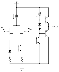
@periblepsis has suggested a handful of neat ideas, including a nice topology for a simple feed-forward preamp. I can see it containing some constant current sources... looks like a really nice circuit, albeit marginally incomprehensible to me in all the details (I'm too young, and a hobbyist).

As mentioned, I'm past the stage that "trivial is good". I'd suggest using a handful of discrete BJT's to implement a minimalistic op-amp topology. Gives you quite a bit of self-adjustment of the various operating points, a negative feedback to help you set the closed-loop gain and frequency response, and quite a bit of "power supply rejection" (immunity against feedback and EMI ingress via the PSU).

I'd use one op-amp-like circuit for the preamp, and another one for the power amp - to stick to your assignment, to follow the usual "macroscopic modular arrangement of gain blocks", and to have some room to tilt the gain this or that way.

There's a free online PDF book that I'd like to recommend: Designing Analog Chips by Hans Camenzind. Mentioned to me before, by others here at SE. You can probably skip all the silicon doping and etching for the moment. I am referring specifically to chapters explaining these topological building blocks:

  1. the long tailed pair
  2. the constant current source
  3. the current mirror

This will allow you to study the most basic op-amp internal topologies and come up with discrete-based circuits along those lines of your own, as a starting point. See for instance this simplified topology or this practical example, allegedly a TL082 When trying this with discretes, you may need to throw in a resistor here and there - although surprisingly the self-biasing circuits often need very little in the way of extra resistors. To prevent premature release of smoke, exercise in your simulators.

In the preamp block, the output stage should work just fine in class A = open emitter into a pull-up resistor, or into a constant current source, or some such. The required output impedance and amplitude mean that neither heat nor current gain are too much of a concern.

As for the power amp: The complementary class AB output stage that you have suggested - looks nice in principle. Next, you need a voltage gain stage to drive it. The simplest would possibly be a single N-BJT connected with common emitter, working into a P-BJT constant current source. Or, rather than a stand-alone CE N-BJT, I'd suggest to use the open collector output of a differential input stage = combine a long-tailed pair, with a current mirror to couple its output to the bases of your Darlington power stage (you can flip N- and P-BJT polarities to correspond to your previous stages).

Also, the cascade of diodes between the darlington bases (to bias the quiescent current of the power stage) seems like a bit of an overkill... Are they schottky? Principally, each B-E junction (two of them in series in each Darlington) should correspond to a somewhat open Si diode, so like 4 Si diodes (1N4148 ?) should have a forward voltage drop roughly on par with your power transies.

I've seen a design where this cascade of diodes was replaced by a single N-BJT connected in "common emitter" basic topology, with a trimpot between C/E, the adjustable pin connected to the Base - allowing you to adjust the quiescent current of the power Dalington totem. (Use a multi-turn trimpot, and start with the Base pulled all the way to the Collector, for minimal voltage between the Dalington bases.) If you thermocouple this "bias setting helper BJT" to the power darlingtons, you get automatic quiescent current adjustment to prevent thermal runaway.

Further sources of inspiration: 1 2 3 - ordered from the simplest to the most comprehensive. This is not to humiliate you, or to suggest that this is the way to go - I mean to suggest that you try to find repeating concepts, circuit stages and tricks in each of those amps. All of them are your basic class AB with a diff input, just with a different "depth of attention to detail".

Note that the Darlingtons have some forward voltage drop from B to E, especially when you drive them to seriously open. And you need some more "voltage headroom" for the stage that's driving the Darlington bases. You should strive to squeeze the most out of that little "headroom near the rails" - by using a current mirror against an active constant current source, to drive the Darlington bases. Even that way, the inevitable voltage drops down the cascade of the B-E junctions in the very output, principally limit the efficiency of this style of a power amp. If you have +/-12V to play with, and you need 5V RMS = approx. 7V peak on the output, I believe that this is achieavable without additional radical tuning. (There are designs with CE-connected power output, able to drive "rail to rail", that are however more sensitive to setting the quiescent current.)

Does it feel way too complicated?

Based on my historical early experiments with "simple" circuits, just individual transitors (up to 3 per amplifier block), all I can say is that reducing the transistor count ends up bringing more headache than design clarity. Those "simple" circuits easily end up requiring more tweaking (based on experiment and measurement), and get you stuck in a swamp of compromise and inefficiency, compared to a circuit making use of the "three friends of op-amp magic" listed above.

EDIT:

with respect to the note about using a transformer in the PA, if the lecturer really wants you to dwell on the very basic principles, how audio used to be built like a century ago, maybe try a query into google images along these lines. Note that these old topologies, with a minimum of valves and lots of transformers in the signal path, initially were adapted for / adopted in transistorized designs. In those days, discrete transistors cost an arm and a leg. What was that - sixties? Maybe still into early seventies? Guess what the ratio is today, comparing the cost of a transistor to the cost of a custom transformer. Especially when prototyping.

Next came transformer-less audio PA designs, initially with a single-transistor CE N-BJT feed-forward input and a quasi-complementary output totem. Back in the day, the quasi-complementary output totem was popular for cost reasons, and remains in use in on-chip integrated designs where the process favours N-polarity transistors (P-polarity are difficult or impossible to achieve, or their parameters lack luster).

Overall, class AB with a differential input stage (excess open-loop gain and a negative feedback), is like eighties to nineties. About a decade ago, if not two decades, there's been a massive exodus towards class D in audio PA. Even consumer radio of any kind (long wave to WiFi to 4G/5G) hardly has any near-discrete analog front end anymore. Pretty much everything is done by single-chip solutions using broadband sampling (rather than superhet mixing). You do meet some LNA's and mixing in TV antenna technology (satellite and terrestrial), but that's a swan song.

frr
  • 2,808
  • 14
  • 14
  • You mention ...looks like a really nice circuit, albeit marginally incomprehensible to me in all the details. I'm sure you already understand the current source. And the circuit I proposed doesn't require its thermal stability but jonk writes a decent answer here on the topic. Might be worth skimming over. The NFB divider I'm sure you also follow. This just leaves the two BJT section. But I laid that out in a nice block diagram that I hoped helped some. If you have any questions about any of that, please do ask. – periblepsis Jan 02 '24 at 18:30
  • It's likely modern curriculum has had to sacrifice time spent on outdated linear amplifier design to make time for more modern approaches a student must also have some familiarity. There's only so much time to work with. But engineers still need to have many many tools in their toolbox. (One who only know how to use a hammer will see every problem as a nail.) An analog audio amplifier is still a good place to see if a student has mastered the basics sufficiently well to create/produce something that will work using linear analog methods. Needs for such skills hasn't completely gone by the way. – periblepsis Jan 02 '24 at 18:31
  • I did try to take an incremental approach, beginning with just three concepts: the current source, NFB, and a simple amplifier topology. And use those as a segue into a design that builds on those in a way that is progressive, step by step, towards something that should just work right. I use those as a foundation before adding the remaining two ideas, a VBE-multiplier and a quadrant power driver, to complete a design that met requirements. I believe you already know about these last two, but if I passed you by in some way please feel free to ask. Oh, and +1. – periblepsis Jan 02 '24 at 18:36
  • @periblepsis thanks for all your comments and references to further reading - much appreciated :-) The constant current source with two transistors is not shocking to me. Just the connection of Q9 and Q12 (common emitter, i.e. emitter to the power rail) together with the drivers Q10 and Q11 was a little eye-watering to me at first. Then I realized that this is not much different from a more traditional "darlington cascaded" topology. I'd hazard to call your version "current coupled" (drivers to the power totem). – frr Jan 02 '24 at 22:20
  • It is current feedback (CFB). Elliot discusses that here. Good catch! Feedback is to the low-impedance emitter. – periblepsis Jan 03 '24 at 00:20