Not just that the output is ~0.7V below (when high), but the gain is strictly lower. That is, even if we add back the voltage offset (using a complementary pair), the change in voltage at the output is smaller than the input:
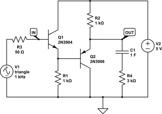
simulate this circuit – Schematic created using CircuitLab
(Also showing an AC load, C1+R4, to approximate the load due to subsequent gate inputs or transmission lines.)
Since it's a linear circuit, we don't need to confine ourselves to square waves alone, and a triangle wave lets us see the nuance of what's going on here.
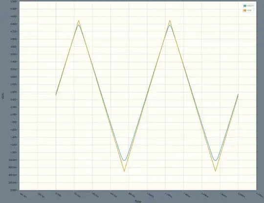
Notice the slope is more shallow at the output than the input. No matter how many we connect in a loop, loop gain is less than one, the signal decays, and it "forgets" what it was doing.
The peaks are also especially shortened, meaning we should expect extreme values to decay even quicker. Granted, such extreme values might not be typical of real RTL (resistor transistor logic) applications, that this kind of circuit might fit into. More modest logic levels are usually chosen: real RTL, DTL and TTL ICs chose values near <20% (low) and >40% (high) of VCC, give or take.
Now, you might claim that there's something unfair about this circuit, perhaps it was constructed specifically to illustrate the problem, and maybe there's another way to do it, if only we were clever enough. But if we confine ourselves to three premises,
- Resistive input (Thevenin equivalent source)
- Common-collector (or drain) amplifier, with any emitter bias network having positive real impedance
- Resistive output (Thevenin equivalent load)
- Well-behaved input and output impedances: preferably R || C or R + L equivalents, and preferably with Zin large, and Zout small
then we will always and only have gain less than 1.
In particular, we might further stipulate that the input characteristic should match the output, give or take a ratio, because we will never have a source impedance less than a single pin driver of the same gate technology, and it can be higher due to fanout (multiple inputs loading a single output, each input sees effectively a larger source impedance).
We could consider modifying some of these assumptions. We could even, in principle, modify the device itself in some way:
- A negative resistance bias network might afford gain slightly above one (for the same reason that a positive resistance causes gain slightly below one)
- If we break the collector connection from GND/VCC, we can obtain inverting gain from it, and connect another inverter to make higher positive gain
- Early effect (i.e., the collector-output incremental characteristic) causes gain reduction, in a similar way to emitter load resistance; if it can be controlled by design parameters, perhaps it can be made very high or indeed negative. Some devices come close: SiGe HBTs, IIRC, have, or can have, negative Early voltage.
We could further allow additional stages in the circuit, or feedback to the input (which won't play well with fanout, or connecting long transmission lines to it; that is, making Zin negative -- ill behaved), but we can't go anywhere without adding stages, or making things harder to use.
There is one hope: if we allow transformers as passive components, and concern ourselves strictly with the number of transistors or other nonlinear / active / semiconductor devices, then at least at AC, we can obtain positive feedback (for example between C and E, effectively making a common-base amplifier with respect to the feedback path), and at least over whatever frequencies we count as "AC", we can obtain bistability. This would be, I guess, a lot like dynamic RAM, but magnetic in nature, and instead of leakage current decaying the bit values over time, we get flux accumulating in the transformer over time, which will again have to be reset periodically.
We can model an ideal transformer in SPICE, and, I guess I should add that as example to illustrate -- but, true DC transformers aren't exactly trivial in the real world, so it certainly fails in practical terms. (There are a few other practical reasons why transformers don't integrate well, or, at all really, and hence we use capacitors in DRAM.)
The most basic example, as a real circuit, is the blocking oscillator. It's either triggered and conducting (accumulating flux in the transformer), or off. Real transformers can't handle unlimited flux, so the real thing is at best monostable: it can be triggered, then latches on for some time, before turning off.
We might also consider the alternative restriction, the one-transistor memory cell.
I won't go into others here, but since I've brought up transformers, there's an esoteric, but mostly silly, case that could apply:
You can use a single transistor as a negative-resistance element, and make it oscillate multiple resonant tanks at once. Then, introduce some... injection locking, perhaps? Do it such that the phase of each resonant circuit becomes bistable, thus storing, in fact, multiple bits per single active device, in sync with some clock frequency (and harmonics thereof).
But, this is a huge pain in the butt, and needless to say, very hard to make one circuit stable, let alone a computer's worth of them! :)
(Multi-resonant oscillators did, in fact, get brief application: IIRC, early DTMF phones used such an arrangement, in the early days where transistors were still more expensive than the array of transformers/coils/capacitors required to implement, but cheaper than trying to make a vacuum tube that could somehow be powered by phone line bias alone.)


