0

I have the following schematics to amplify a current signal modulated at 10 kHz. The first stage is a transimpedance amplifier with a -3dB bandwidth of 72 kHz. The second stage is a high pass filter with a -3dB bandwidth of 0.13 Hz. The purpose of the high pass filter is to eliminate a possible unwanted offset in the input signal.

enter image description here

However, when I simulate this in LTspice, I obtain an unexpected behavior, as shown in the following image:

enter image description here

The green plot here is the signal before the high pass filter stage, which in this case is centered at zero, as expected. However, the blue plot, which is the voltage after the high pass filter, acquires a negative offset. Why does this happen? Is there an intuitive explanation on why this is the case?

Note: U28 is OPA828 and U31 is NE5532

  • But notice that U31 will also amplify any DC offset present at the input. For example, the NE5532 input bias current is typically equal to 200nA. Thus, DC offset at the input is around 200mV. And this DC voltage will be amplified by the U31 voltage gain. So it is not wise to use a 1Meg resistor and bipolar input opamp. So the LTspice result is too optimistic, or poor NE5532 model used, because the output DC offset will be larger in real word. – G36 Nov 28 '23 at 17:34
  • A quick fix would be to make r138 equal to r134 so that the input current makes an equal voltage on both inputs. Right now that huge 1 meg resistor is killing it. – user1850479 Nov 28 '23 at 17:49

1 Answers1

4

The NE5532 isn't good for these types of low-offset output voltage applications. There are several pointers in data data sheet: -

enter image description here

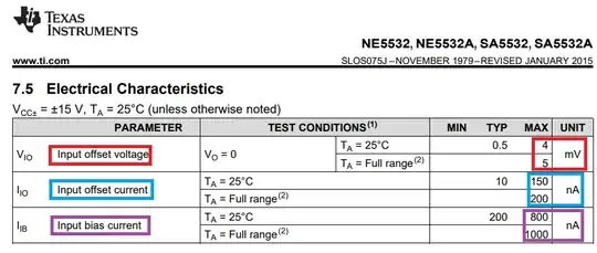
Input offset voltage

At your maximum gain (set by R169) of about 20, a typical input offset voltage of 0.5 mV will produce an output offset error of 10 mV. Far, far worse if the offset is not close to typical. I mean it could be as high as 4 mV at ambient temperature.

Input bias current

Input bias current will flow into R138 and typically, will produce an effective input offset voltage of 2 volts. This gets amplified and too bad, the op-amp output hits the end stops.

Input offset current

The data sheet gives you this figure to help you decide the final error due to bias currents. Input bias currents can be largely cancelled in many BJT op-amp circuits by using matching resistors in both inputs but, offset current tells you how far this can work. With a typical offset current of 10 nA and a resistor of 1 MΩ (R138), the effective error voltage at the input could still be 10 mV and, with your gain at a max level of 20, the output offset would be 200 mV.

What you should consider doing about offset/bias currents

Maybe try using a capacitor in series with R134; this makes the DC gain of the final stage unity. Of course, the capacitor has to be big enough so as not to reduce gains at low frequencies. If 20 Hz is your lower range you would need a capacitor of 2.2 μF in series with R134.

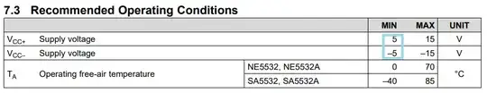
Recommended power supply minimal value

You are running it at +/- 4.5 volts but, the minimum recommended supply is +/- 5 volts: -

enter image description here

How to determine what's a suitable op-amp

Andy aka
  • 456,226
  • 28
  • 367
  • 807