3

Some standard cell libraries include cells optimized for zero wireload capacitance. When might these be used?

Are these used when the output drives a gate that's physically very close to the output? I would have thought that even then, the driving gate should be optimized for something higher than zero.

Tim
  • 131
  • 2

3 Answers3

1

This is one of those nonsense areas you run across. Inside an IC there is very minmal inductance, so you end up with delays that are dominated by RC's and not RLC's. If you have RLC you get wave equation propagation and thus must deal with transmission lines and reflections etc. But the same PDE's (Partial Difference equations) when used with RC result in the diffusion equation and you don't get transmission lines (except in very rare cases with very long runs).

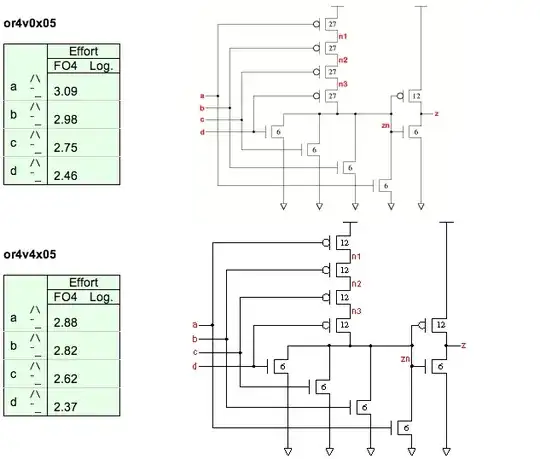
In fact pop by this page and look at the V4 driver which is "optimized" for zero wire load. The O/P drivers are identical to the the other minimal drive device, which indicates that there is no matching taking place. The only real difference is that they've reduced the P Widths in the logic cell so that the \$T_{rise} T_{fall}\$ is no longer matched.

The lower cell is the "optimized" one (snip taken from that link):

enter image description here

Having a cell like that might be useful, but not for the stated reasons. Capacitance is capacitance is capacitance wrt to how you drive it.

I would look into the cell and check out the transistor sizing's to make sure they haven't done something funky.

placeholder
  • 30,170
  • 10
  • 63
  • 110
0

When the gates are physically close together, the wire load is very small compared to the loading of the gates themselves (the transistor gate capacitance). For practical purposes the wire load is zero.

Joe Hass
  • 8,487
  • 1
  • 29
  • 41
  • I don't know what you mean by "close together", but the technology has long since crossed the point where the RC delay of wires could be ignored. – Vasiliy Aug 11 '13 at 00:12
  • @vasily-zukanov Sorry, I disagree. I didn't say that all wire delays could be ignored, but when two standard cells are physically adjacent and the output of one drives an input of the other, then the capacitance of the wire is small compared to transistor gate capacitance and wire resistance is small compared to the effective resistance of the driving transistor. Therefore, the wire RC delay is negligible. – Joe Hass Aug 11 '13 at 01:24
0

Back in the past, the wire capacitance could be neglected as compared to gates' capacitance. However, today this is no longer true.

Now, when you say that the cell is optimized for zero wireload capacitance, I can think of two totally opposite optimizations:

  1. The cell could be optimized under assumption that the post layout capacitance of the wires is negligible.
  2. The cell could be optimized with understanding that post layout capacitance won't be negligible, but that synthesis tool will use a zero wireload model.

The first option is bad. If you use cells that do not account for wires' RC delays you'll get optimistic synthesis timing. Once place and route will be completed you'll probably have many paths that do not meet timing. Depending on the post synthesis tools you have access to, these timing problems can be anywhere from "I don't give a s*** - the tool will do most of the work" to "f***, it'll take me a century to close timing". I'd avoid using these models at all, unless there is solid proof that this won't screw you up.

The second option is not that bad. If you assume that the synthesis will use a zero capacitance wireload model, you can compensate for this optimistic assumption by adding additional capacitance to cells themselves. I'd say that guessing that wires' capacitance will be equal to basic NAND2 capacitance is a good guess. If you indeed run synthesis tool with zero wireload model, this additional capacitances will prevent too optimistic netlist. If you run synthesis tool with non-zero wireload (with post P&R extracted values), the synthesis will not use these cells at all. However, I never heard of anyone who used this approach.

Zero wireload in general:

It is almost impossible to come up with a decent wireload model nowadays. Even custom models will give you just a rough estimation. The only way to close timing on today's designs is to extract the RC load post place and route. This fact led to a conception of "fast synthesis" - synthesize for the first time with wireload zero model, perform place and route, extract RC, feed the extracted RC back to synthesis tool and re-synthesize.

Sometimes during "fast synthesis" the uncertainty of the clock period is specified with higher value than required. This is the way to compensate for lack of interconnect delays.

However, I never heard that the cells themselves were changed in any way for the purpose of the above flow.

RC prediction during synthesis:

There were many attempts to come up with an algorithm to predict RC delays for each individual cell. I don't know how accurate these algorithms are. There is a high cost associated with these tools (for example: "Topological" Design Compiler by Synopsys is more expensive than usual DC; considerably more).
Vasiliy
  • 7,443
  • 2
  • 21
  • 38
  • Standard cells designed for zero wire load use smaller transistors, which reduces power consumption. Standard cells designed for higher loads use bigger transistors. All cells are characterized over loading, temperature, and input rise/fall time. The synthesizer does in-place optimization (IPO) to select the best version of each cell, based on the extracted wire loading and the criticality of the timing path. A good cell library will have a multitude of sizes for each cell type. – Joe Hass Aug 11 '13 at 01:33
  • @JoeHass, When saying "extracted wireloading", do you refer to extraction from post P&R? I know that the wireload model is specified per module (usually based on its size), but I've never seen a synthesis tool which calculates the required wireload per cell. However, I know that DC has Topographical feature which seems to be also related to RC predictions. Maybe you're referring to this one? Anyway, using zero wireload model is a bad idea and leads to over optimistic timing. – Vasiliy Aug 11 '13 at 17:55
  • It's been a while since I did this, but Synopsys has P&R tools (Astro?) that will extract loads for every net after P&R and then do in-place optimization to swap low drive cells for high drive cells. I agree that using a zero wire load model should not be used for designing circuits, but that's not what the original question was asking. It does make sense to have some cells that are optimized for zero load, as long as you have functionally equivalent cells with high drive. – Joe Hass Aug 12 '13 at 00:46
  • @JoeHass Ok, now I understand what you're saying. You're assuming that these cells which were "optimized for zero wireload" will be used by synthesis tools during post P&R iterations, right? Whenever the extracted RC will be low enough, these cells will be used. Don't think "zero wireload" term is appropriate here - I call these cells "usual cells" and all others "high fan-out cells". – Vasiliy Aug 12 '13 at 07:39