For a proper dc current gain, how do i choose a proper q point without getting the transistor into saturation or cutoff using voltage divider bias technique?
Asked
Active
Viewed 167 times
0
imran muhd
- 339
- 7
3 Answers
3
I've already spent time telling you how at this answer. But let's do the same thing but now with these curves.
Let's consider the case with \$V_{_\text{CC}}=12\:\text{V}\$ and where \$I_{_\text{C}}=9.2\:\text{mA}\$ when \$V_{_\text{CE}}=0\:\text{V}\$. While the circuit I'll use is a standard common-emitter arrangement, it turns out that for pretty much any arrangement you will need to DC bias the BJT, similarly. So it's a good textbook case to analyze. Here's the typical schematic:
simulate this circuit – Schematic created using CircuitLab
Let's select an NPN BJT -- the 2N2222 with a typical forward beta of \$\beta_F=200\$ and a \$V_{_\text{BE}}=674\:\text{mV}\$ when \$I_{_\text{C}}=2\:\text{mA}\$. (I extracted this from the LTspice standard model for the 2N2222 device model.)
Let's also use your situation where \$R_{_\text{C}}=1.2\:\text{k}\Omega\$, \$R_{_\text{E}}=100\:\Omega\$, and therefore \$I_{_\text{C}}=\frac{V_{_\text{CC}}}{R_{_\text{C}}+R_{_\text{E}}}\approx 9.231\:\text{mA}\$ when \$V_{_\text{CE}}=0\:\text{V}\$.
If we plot all this out:

Then we might choose to set the quiescent point for \$V_{_\text{CE}}\$ at \$6\:\text{V}\$. This means that the quiescent \$I_{_\text{C}}\approx 4.5\:\text{mA}\$. If so, then the quiescent \$V_{_\text{E}}=100\:\Omega\cdot 4.5\:\text{mA}=450\:\text{mV}\$ and so the quiescent \$V_{_\text{C}}=6\:\text{V}+450\:\text{mV}=6.45\:\text{V}\$. Now we find that \$V_{_\text{B}}=450\:\text{mV}+674\:\text{mV}+26\:\text{mV}\cdot \ln\left(\frac{4.5\:\text{mA}}{2\:\text{mA}}\right)\$ or \$V_{_\text{B}}\approx 1.145\:\text{V}\$.
From that and the rule of 10, we should find that \$R_2=\frac{1.145\:\text{V}}{\frac1{10}\,\cdot\,4.5\:\text{mA}}\approx 2.544\:\text{k}\Omega\$ and that \$R_1=\frac{12\:\text{V}-1.145\:\text{V}}{\frac1{10}\,\cdot\,4.5\:\text{mA}+\frac{4.5\:\text{mA}}{\beta_F=200}}\approx 22.974\:\text{k}\Omega\$.
Let's Spice this idea:

That's very close to prediction. So we can call it good except for the fact that the base pair isn't standard resistor values. If we pick things out of E24 (5%) then we'd say \$R_1=22\:\text{k}\Omega\$ and \$R_2=2.4\:\text{k}\Omega\$. In this case, we'd find:

Close enough, I think.
periblepsis
- 8,575
- 1
- 4
- 18
3
Basic idea
This is not a specific transistor circuit idea only. It is a general idea that can be seen everywhere around us where some quantity oscillates. Obviously, to get the maximum deviation in either direction, we have to choose the zero (quiescent) value in the middle of the range.
Implementation
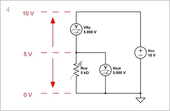
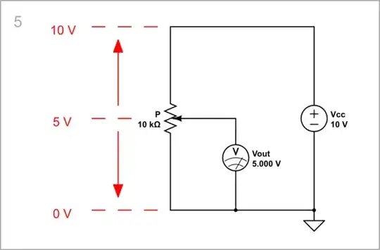
In circuits, we can see it in voltage amplifier stages. They consist of two devices connected in a voltage divider configuration - one of them ("pull up") is connected to Vcc, and the other ("pull down") to ground. Usually, in the simple amplifier stages, the pull-down device is the "amplifying" device (it is grounded). With the series of CircuitLab experiments below, I will show that no matter what is there, the idea and the end result are the same - if we set the quiescent voltage in the middle (5 V), the output voltage has a maximum swing. For this purpose, I have included as a pull-up device a "visualized resistor" Rc with a resistance of 5 kΩ (i.e., a voltmeter on which I have deliberately reduced the resistance to 5 kΩ), and as a pull-down device I have put several types of devices such as:
Transistor...
Here I have driven the transistor with a (bias) current source Ib to obtain a linear function Vout = f(Ib). I have set the quiescent voltage (5 V) as follows:
I open the Ib parameters window and start changing Ib watching the Vout voltmeter until it shows 5 V. As you can see, a rather "ugly" value of 6.691 μA is obtained. We can even calculate the transistor beta - β = 1000/6.691 = 150.
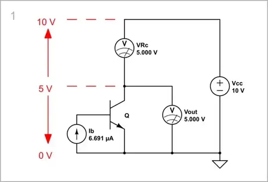
simulate this circuit – Schematic created using CircuitLab
Let's now sweep Ib to see the graph of the transfer curve Vout = f(Ib). The limits in which to change Ib can be established experimentally (0 ÷ 14 μA). As you can see, the curve is almost linear.

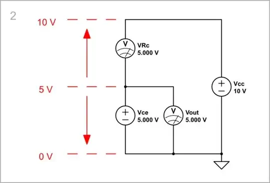
Voltage source...
For the purposes of this topic, we are only interested in the collector voltage, and not how it is produced. Therefore, although it seems a bit paradoxical, we can replace the transistor with a voltage source directly producing this voltage.
As you can see, the curve is linear and the same as above.

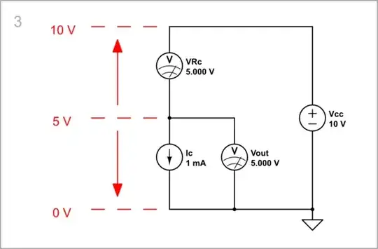
Current source...
Of course, a current source Ic best resembles transistor behavior. It creates a voltage drop VRc = Ic.Rc = 1 mA.5 kΩ = 5 V across the collector resistance Rc, and the quiescent voltage is 5 V.
The curve is absolutely linear as above.

Variable resistor...
An ohmic resistor is a poor approximation of the transistor because its resistance is linear, but it does a good job for our purposes.
Now the curve is non-linear but as we already said it does not matter to us.

Potentiometer
Modern transistor amplifiers are usually made with two complementary transistors. For our purposes we can emulate them using a potentiometer.
The result is the same - 5 V quiescent voltage and an absolutely linear curve.

See also my story about load line.
Circuit fantasist
- 16,664
- 1
- 19
- 61
0
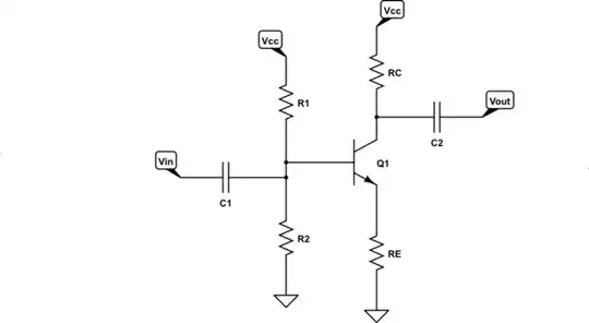
The Q point (quiescent voltage at the collector) would normally be chosen to be Vcc/2. You might choose a voltage to be slightly higher than Vcc/2 to allow for the voltage drop across the emitter resistor (RE). This then enables the collector voltage to swing equal distance in either direction when the transistor is driven by an ac signal at the base and so saturation and cut-off occur at the roughly the same output amplitude. This approach maximises available output amplitude swing.
For a common emitter amplifier it is voltage gain that we are interested in. The current gain between base and collector is determined by the beta of whatever transistor we choose to use.
The topology of the common emitter amplifier tends to allow for beta variation between different transistors by keeping the effect of beta variation on the dc biasing low.