BJT Small Signal Analysis
Image below taken from page 4 of this reference:
http://www.iitg.ac.in/apvajpeyi/ph218/Lec-8.pdf
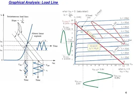
Input Dynamic Load Line Analysis
The input load line analysis is shown on the left side graph. The DC Q point is set by the bias design and the AC variation depends on the magnitude of the AC input signal.
Output Dynamic Q-Point Load Line Analysis
The output load line analysis is shown on the right side graph. The Q-point is constrained to a location on the output load line. The axis shown represent the value for these variables of interest:
$$I_C, V_{CE},I_B$$
with the assumption that the AC small signal input waveform is a sinusoidal waveform.
Note the vertical axis refers to the collector current in units of ampere. The horizontal axis refers to the collector-emitter voltage in volts. The product of current and voltage is power given in watts. One can draw an operating point vector with the tail at zero (origin) and the head at the Q-point. Then the collector current is the projection of this vector onto the vertical axis and the collector-emitter voltage is the projection of this vector onto the horizontal axis. The area under the dynamic Q-point, based on these projections, is the power dissipation in the output side of the transistor at a point in time. The maximum voltage, current, and power ratings for the transistor would be given by a safe operating area (not shown in the curves above).
Note the diagonal base current axis and the characteristic curves for constant base current are overlays placed "on top of" the horizontal and vertical axes used for output load line analysis. If drawn to scale the collector current would be the forward current gain times the value indicated as constant base current in the characteristic curves. The proper way to interpret either a voltage or current axis along the load line is that is it is a separate graph of physical properties superimposed on the output graph at an angle so its vertical axis corresponds to the load line.


