2

I am working on understanding the NAND conversion. I have just got the basics of two-level NAND conversion, and when I went to the book example for a multi-level NAND conversion it used solved an example until reaching to a level and kept the OR gate symbol, although he could replace it with NAND. I have searched on the web I found some people done the same but without reasoning why. I read the text book related-material but also the writer didn't explain why he left it.

The example is:

(a) is the initial (b) is after simplifying (note the B')

Why did he leave the OR gate symbols although he could replace them with NAND?

greybeard
  • 1,794
  • 1
  • 7
  • 20
Mhd Ghd
  • 29
  • 1
  • 3
    The two different symbols in the bottom diagram represent exactly the same gate -- a NAND gate. – Dave Tweed Sep 29 '20 at 13:58
  • i mean the 2nd and 4th levels (OR's) must be replaced with NAND why he left them @DaveTweed – Mhd Ghd Sep 29 '20 at 14:00
  • 3
    That's the point -- those are NAND gates. Write out the truth table and you'll see this. – Dave Tweed Sep 29 '20 at 14:01
  • 1
    i know they are equivalent to NAND gate but why we don't put a NAND symbol instead ? @DaveTweed – Mhd Ghd Sep 29 '20 at 14:02
  • @Andyaka the goal is repressent the equation using NAND's the first part repressented the equation as it is the secound supposed repressent it with NAND – Mhd Ghd Sep 29 '20 at 14:04
  • 1
    We don't put the NAND symbol because it would make the diagram harder to read. Why do you think that this is a problem? – Dave Tweed Sep 29 '20 at 14:16
  • @DaveTweed from my opinion I might say it because we can visualize the De Morgan's Theorem if we kept it like this. however, really thanks to you i felt like i am getting the point now. – Mhd Ghd Sep 29 '20 at 14:52
  • 2
    Anyway, I find it irritating that B of the first circuit changed into B' of the second circuit. First I thought this is an error... until I saw that little tiny tick. I would have inserted a NAND as inverter. -- Lesson to learn: Things done by humans tend to be inexplicable. ;-) – the busybee Sep 29 '20 at 15:03
  • 1
    However, seeing the inverters at the output and at the input of the same wire demonstrates the correct transformation. The author could have added a third circuit where these input-inverted-OR symbols are replaced by NAND symbols. – the busybee Sep 29 '20 at 15:05

2 Answers2

2

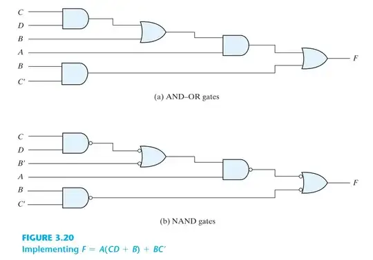
The two OR gates you see are negative logic, which has the same truth table as NAND. DeMorgan's Theorem tells us so.

That is,

  • Negative-logic (Demorgan) OR: Y = !A + !B

is the same as:

  • positive-logic NAND: Y = !(A & B)

Work out the truth table for each, you will see that they are the same.

What the authors intent seems to be is to convey is that if you have choices for the signal polarity (notice in the second diagram they use B' and C', that is, negative-true inverted versions of them) then you can use Demorgan's Theorem to simplify your logic somewhat - if 'simplify' means use all NAND.

As to why they chose to represent the two OR gates as neg-logic OR instead of pos-logic NAND, they seem to want to show similarity in structure to the original logic. That is, those neg-logic ORs occupy the same functional space as the pos-logic ORs in the original diagram.

In the bigger picture, they're encouraging you to think about negative-logic and positive-logic representations of the same gate.

By the way, the same DeMorgan conversion can be done using NOR (neg-logic AND), as was famously done to build the Apollo Guidance Computer. That said, for CMOS there is area and leakage advantages that favor using NAND over NOR. More here: Why is NAND gate preferred over NOR gate in industry?

However, real-world logic used in ASICs and other ICs won't use just one gate type, be it NAND or NOR. Instead, they will use a variety of structures provided by the standard cell library, including efficient and-or-invert (AOI) / or-and-invert (OAI), transmission gate types, as well as custom cells for critical and complex paths like RAMs, ALUs or multipliers. More here: What is the lowest level of CPU programming above transistors?

hacktastical
  • 53,912
  • 2
  • 49
  • 152
0

enter image description here

These two gates act as an NAND gate example: lets consider gate 1 marked in the figure lets take A as one input B as other input

now, since there is a bubble input of or gate will become A' and B'

so, (A'+B')' after simplification it will be => (AB)' This is nothing but NAND gate output

this is the reason in your image they are using or gates whose both inputs are complimented.

  • I think the question is asking why one would use OR gates instead of NAND in the sense that one presumably performs better than the other, and what is that reason? – Null Nov 16 '21 at 12:24