Can anyone show me a simple circuit to shift a 0V/5V square wave (low freq, under 10Hz) to a square wave -10V (when was 0) to +10V (when was +5V). Can it be done with some transistor or do I need an opamp?
Asked
Active
Viewed 4,288 times
1
-
Is the duty cycle always 50%? – The Photon Jul 14 '17 at 21:28
-
Actually not, the duty cycle can be any – Dimitri Petrucci Jul 14 '17 at 21:43
-
4 BJTs could do it. How much current can the source supply? How much current must the output supply? – jonk Jul 14 '17 at 23:02
-
@DimitriPetrucci, that's important information. You should include it in your question (not just in the comments). – The Photon Jul 14 '17 at 23:07
-
Also, if the input voltage changes, for example, becoming a 1 V to 3 V square wave, do you want the output to change proportionally? And what power supply voltages do you have available? – The Photon Jul 14 '17 at 23:16
-
5The simplest way to do this is using a MAX232 level shifter. You don't even need a ±10V supply, it's on-chip. – Janka Jul 15 '17 at 00:32
-
1@Janka, then how do you beef up the charge pumps to +-10 V? Nominal output is +-7 V. – Ale..chenski Jul 15 '17 at 02:32
-
I go back to the source of this question and check whether I really need ±10V. I doubt it. – Janka Jul 15 '17 at 02:37
5 Answers
11
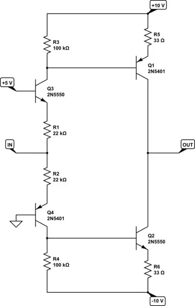
Opamps are the universal answer to everything today. They are reasonably priced, precise, widely available, can provide rail-to-rail input and output, etc. But since you added "some transistor" and since MOSFETs are more pricey, by and large, than BJTs and have their own unique foibles, I'll give a simple BJT solution that is really easy to understand.
I've added no "speed-ups" to it, since your specification says "under \$10\:\textrm{Hz}\$." I've also avoided adding reverse voltage \$V_{BE}\$ protection diodes for any of the transistors. I don't think that will be an issue for you, more especially because I didn't add any speed-up caps. I'm going to also assume (it's reasonable, given the question) that you have the following rails: \$+5\:\textrm{V}\$, \$+10\:\textrm{V}\$, \$-10\:\textrm{V}\$, and a common ground (obviously) that they all share.
Finally I'm going to make some assumptions: (1) that your source can handle \$\ge 200\:\mu\textrm{A}\$, both source and sink; and, (2) that you can accept an output that won't need more than 20-30 times that, or so. (This depends upon the actual output BJTs you use and just how "saturated" you want them.) So you should NOT use a load of more than about \$2\:\textrm{k}\Omega\$ when using the exact values I'm providing. If your load will be heavier than this by some factor \$X\$, you'll need to reduce the values for \$R_1\$ and \$R_2\$ by that same factor \$X\$ and your input source will need to be able to sink and source \$X\$ times what I mentioned above, as well. (Oh, and you can remove \$R_5\$ and \$R_6\$, if you want. They are not essential. If you keep them, also adjust them by the same factor \$X\$ you used to adjust \$R_1\$ and \$R_2\$.) The values for \$R_3\$ and \$R_4\$ aren't critical. You can leave them unchanged, or change them, accordingly.
I'm using somewhat higher voltage BJTs for the output. I just figured I'd make this capable of much higher rail voltages, in case anyone cares. Feel free to replace them as you see fit (with small signal BJTs like the 2n3904 and 2n3906, if you want.)
Feel free to jump to the bottom, where probably the better answer is located. I present a few steps in getting there. But if you are in a rush, just skip all of it and go there.
Now to get started with a direct approach:
simulate this circuit – Schematic created using CircuitLab
Above, I completely ignored your suggestion that \$0\:\textrm{V}\$ on the input generates \$-10\:\textrm{V}\$ on the output. Instead, the above circuit will put \$+10\:\textrm{V}\$ on the output with \$0\:\textrm{V}\$ on the input and will put \$-10\:\textrm{V}\$ on the output with \$+5\:\textrm{V}\$ on the input.
But it's easy to explain. The input source either "pulls down" on the emitter of \$Q_3\$, which sinks base current of \$Q_1\$, turning \$Q_1\$ on; or else it "pulls up" on the emitter of \$Q_4\$, which sources base current into \$Q_2\$, turning \$Q_2\$ on. That's really about all there is to it.
If you don't like the polarity, though, you can place an inverter at the input, like this:

Kind of brute-force, but it gets the job done. But if you need more drive capability in the original circuit, then the added inverter in this latest circuit will also need to be modified. Just a warning.
I'm not going to spend any more time on this one except to say that it points up how you might modify someone else's circuit to get the polarity you wanted. On to the next step.
To avoid the inverter and to arrange things to get the output polarity you asked for, you can try this:
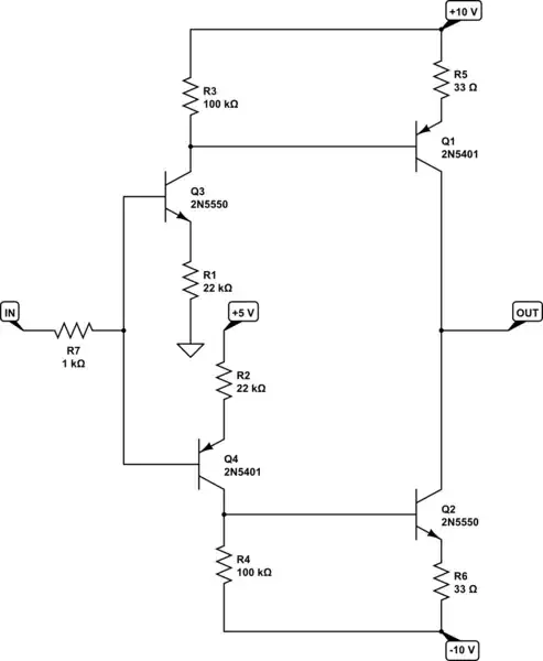
This is actually probably better still and it provides the polarity you asked about. I've added a series resistor, \$R_7\$, just in case there is any concern about oscillation around the transition edges.
It works in a similar way, though now the input source directly drives the bases rather than pulling on the emitters. But it also doesn't load down your input source nearly as much. So that's why it's probably better for typical uses.
But there's a small problem with it, too. Before I talk about that, a short note:
Just be aware that the above designs are not meant to be operated linearly. A square wave input will be fine, because the transitions are fast. (Sure, I've added some emitter degeneration just in case. But it's still not a good idea to operate them with slow rise and fall times.)
Okay. Now back to the small problem.
The values for \$R_3\$ and \$R_4\$ are weak in the above diagrams. They perform several functions (cheaply), but one of them is to help with the transitions.
There's a base-collector capacitance for all BJTs, but in the case of this topology the base-collector capacitance for \$Q_3\$ and \$Q_4\$ are the problem. When the input pulls one way (or another) at the base of one of these two BJTs in order to turn it off, then this small capacitance also pulls similarly on the bases of \$Q_1\$ and \$Q_2\$ causing them to momentarily increase their collector currents just prior to turn-off; right at the same moment when the opposing transistor (\$Q_2\$ or \$Q_1\$) is turning on. This is not so good, as it connects the power rails together through the two output BJTs for a short moment and that wrecks some havoc. (It might only be for a couple of microseconds. But it's worth seeing if it can be reduced or removed.)
If you can afford the extra currents in the driver BJT stages, you could simply reduce the values for \$R_3\$ and \$R_4\$ to strengthen them a bit to supply the needed transition currents more readily. This reduces the time period and therefore the peak "short-circuit" currents, lost power, and attending havoc. But I set them very weak here, as it doesn't matter as much as one might hope. Still, you could cut them down by a factor of 10. But the problem, while smaller now, would still be present.
Another (better, I think) approach would be to instead add one small capacitor as shown below:
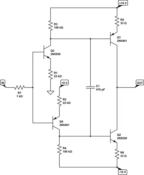
This works because just about the only node moving upward in voltage when the input is driving downward, is the base of \$Q_2\$. (The reverse concept is also true.) By tying a capacitor between those two nodes, the turn-on of one side aids the turn-off of the other side. This compensates for the base-emitter capacitance on both sides and nearly eliminates the spikes during the transitions.
The value of the capacitor needs to be sufficient to overwhelm the base-collector capacitance of \$Q_3\$ and \$Q_4\$ (which are different for various BJTs) and the value I've added is large enough to handle several different BJTs you are likely to encounter. But it could be still larger as it's not critical as it has access to substantial currents.
jonk
- 77,876
- 6
- 77
- 188
-
1Have you considered the cost of your proposal as compared to a single OPAmp? For example, the Toshiba TA75S558F (+-18 V 40 mA, 3 Mhz) price is $0.44@1ea. at DigiKey, while 2N5401/2N5550 are $0.23 -$.46 each ($1.50), plus resistors, board space, plus soldering. Is this worth doing? – Ale..chenski Jul 15 '17 at 15:50
-
1@AliChen I'm a hobbyist. I volunteer/teach HS students every year. I give away BJTs like popcorn because I have buckets of them (over 22,000 new ones) and they cost me about 0.3 cents each. Each student will get a handful so they can play on their own and learn. I can't do that with opamps. The price just isn't there. Besides, the OP here brought it up and I gave a nod to it in the first paragraph. If they hadn't, I would have probably provided an opamp solution or else no solution (depends on my mood.) And there are plenty of pros here who will always reach for an opamp as an answer. – jonk Jul 15 '17 at 16:58
-
1Jonk, I can see your angle. Essentially you are proposing to make the output stage of an OPA from discrete transistors. Obviously this is good for educational purpose and when you have this bulk surplus, but we don't know the real need of OP. – Ale..chenski Jul 15 '17 at 17:47
-
5@AliChen One of the wonderful things about a community like this, is that each of us brings our worldviews and perspectives. And while there certainly are plenty of wrong answers, there are remarkably few 100% right-for-everyone answers. For me, I love the fact that I get to learn from people like you and others who bring their professional and hard-earned knowledge to the table. And once in a while, I also enjoy dropping a small rock in that pond, too. (Perhaps on the shallow end of the pool, though!) Each bit (that isn't simply wrong) and may help just one person someday is good. I think. – jonk Jul 15 '17 at 18:57
6
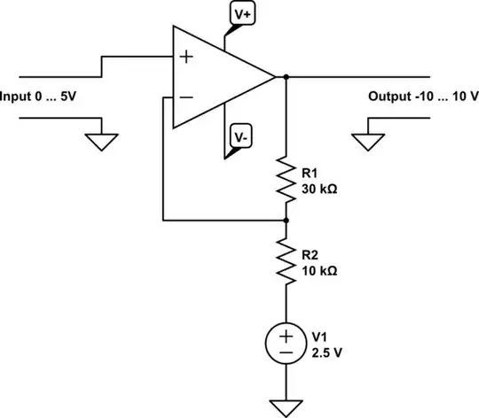
Rather than an op amp, a comparator is a good fit for this. In the following circuit, anything below about 2.5V on the input will give a -10V output, anything above will give +10V. The output of the LM393 is open collector, which makes things simpler than needing a rail to rail op amp.
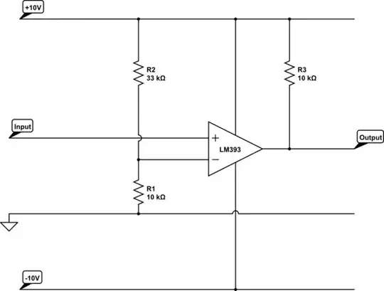
simulate this circuit – Schematic created using CircuitLab
(I made a mistake in the original with the potential divider values. I've updated the schematic)
Ian Bland
- 2,651
- 1
- 14
- 18
-
thank you! I guess it can only be done with LM393? it won't work with a standard opamp since it won't reach -10V and +10V, but something less, right? – Dimitri Petrucci Jul 16 '17 at 12:36
-
Yes, this isn't really a job for op amps in my view, but it is a good fit for a comparator. The big difference is most comparators like the 393 have an open collector output so are well suited to pulling up and down to the rails if required. Most op amps (at least, cheap ones) aren't going to reach both rails easily. This is the simplest solution I'd go for, but then I've got a lot of LM393s already :) – Ian Bland Jul 16 '17 at 16:20
2
Here's one way of shifting it, click here if you want to play around with the circuit.
It's either the upper one or bottom one you'd go with, BJT or MOSFET. Whatever you got.

This schematic assumes that you got all the voltages available, like in a lab power supply. If you however need to make the voltages from 5 volt. Then your question needs to be updated.
Harry Svensson
- 8,169
- 3
- 34
- 53
0
(Having to answer as I can't include a schematic in a comment.)
This is not a practical method, use the discrete transistor suggestions instead. An op-amp is overkill for digital stuff.
But it should work, it's a simple OP amp non-inverting amplifier with a gain of 4 and a virtual ground biased at 2.5 volts. It requires a dual rail supply. The bias voltage source must have a low impedance, you can use another OP-amp as a buffer for a simple resistor divider.
simulate this circuit – Schematic created using CircuitLab
Oskar Skog
- 924
- 2
- 11
- 19
-1
What you need to do is to make a circuit that gives your input signal a -2.5V offset and then makes its magnitude 4 times bigger.
One of my favorite ways of "Shift and Gain" circuits are Op-amp adders.

you can see the circuit's simulation(in PSpice) below:

Farhood ET
- 101
- 2
-
3Check and correct your schematic, there are some things in it that seems odd and incorrect. – Oskar Skog Jul 19 '17 at 10:26
-
@OskarSkog It works fairly well as you can see the result of the circuit's simulation in PSpice that I have appended. – Farhood ET Jul 22 '17 at 14:48
-
1I don't trust that simulation. The feedback loop is output--4ohms--inverting_input--500ohms--virtual_ground giving a voltage gain of 1.008. The input is attenuated by the resistor divider R6-(R5-R4) to 0.444. The total gain should be 0.448. The bias/shift is also a tad off, compare the dividers R2-R1 and R6-(R5-R4), the former perfectly halves the voltage while the latter outputs 4/9. Zero output will occur at 2.8125 volts in, not at 2.5 V. (Not relevant for digital stuff though) – Oskar Skog Jul 22 '17 at 15:46
-
And even if that circuit works, there are a few things you should explain and a few things you should correct: R5 and R4 are in parallel, why not use a single resistor? The gain caused by the feedback loop, it looks like anything but 4. A few extra joints. Why are you attenuating the input? Why use a resistor divider and a 2.5 V voltage source instead of a single 1.25 V source? – Oskar Skog Jul 22 '17 at 15:49
-
See schematic at https://electronics.stackexchange.com/questions/317458/level-shift-0-5v-to-10v-10v#answer-319890 it's simpler and clearer. – Oskar Skog Jul 22 '17 at 16:02
-
@OskarSkog This circuit is better in a way that it is more general, if he wants to add an offset or subtract another one this is the answer. I have implemented this circuit multiple times for signal conditioning for ADCs' input signals or output conditioning of DACs. Although it's much better to use bigger resistances, because of the input or output resistance of the Opamps, this was simulated on an ideal Op-amp. – Farhood ET Jul 22 '17 at 16:26
-
@OskarSkog and he is conditioning a low-frequency signal, which makes Op-amps a very good choice. He doesn't even need to use an instrumentation op-amp which is more expensive. – Farhood ET Jul 22 '17 at 16:29
-
1No, that was not simulated using an ideal op-amp, it was simulated using a surreal op-amp. Have you even looked at your own schematic? 4 ohms between output and inverting input, it's practically a buffer. And there are so many confusing things. – Oskar Skog Jul 22 '17 at 16:41
-
@OskarSkog oh sorry I didn't saw that it was a 4 ohms resistor, thought it was 4k. fixed. – Farhood ET Jul 22 '17 at 16:53
-
Can you explain why you have R5-R6 in parallel, the resistor divider R2-R5-R6, and the resistor divider R1-R3 instead of a 500 ohm resistor to a bias voltage? – Oskar Skog Jul 23 '17 at 17:52
-
@OskarSkog here is how a simple Op-amp adder works, you can prove it via superposition principle. http://i.imgur.com/sfZTv4r.png – Farhood ET Jul 25 '17 at 06:45