You're using net-labels.
Net labels are horrible from a maintainability standpoint. I see at least one net (Bat+), where there is no reason to be using a net label.
Net labels are the schematic equivalent of GOTO. Basically, it lets one point on a schematic connect to any number of other points on the schematic, while not providing any clear indication of how many points it is connected to, or where those points are.
If I am working on someone else's project, and they use net labels, it can be very hard tell what is connected to what, particularly if the schematic is spread over several sheets. Once you have many sheets (5+), it effectively becomes unmaintainable. It's the schematic equivalent of spaghetti-code.
The proper way to manage multiple-sheet projects is unfortunately not available in eagle. It's called Hierarchical Design. Effectively, each schematic page is used as a meta-component, and you have a top-level schematic that describes the interconnections between sheets. This lets you determine everything that is connected to any net, by following the wires. Any wire leaving a sheet only goes to one place, the top sheet. That sheet may have it connecting to multiple other sheets, but it's clearly shown, rather then implicit, as net labels are.
I know you can do this in Altium Designer, and I believe it is also possible in Cadence Allegro, though I have not use cadence much.
To be honest, about the only feature Eagle has going for it is it's cheap. Many of the other EDA packages out there are so much nicer to use, and produce much better looking drawings. I don't think I've ever seen a drawing done with Eagle that wasn't ugly. At best, they're just unpleasant. At worst, they're a god-awful nightmare.
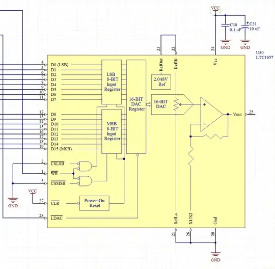
Also, you are drawing your components with the pins physically placed where they are on the actual device.
The whole point of a schematic is to abstract the function of a circuit away from the nitty-gritty details of which pin goes where. Forcing the schematic to physically match the devices makes the schematic messy, and harder to read. The whole purpose of modern EDA software is to let the computer, which is much better at handling all the meticulous details of what wire is connected to what, do the correlations for you.
Generally, you want you Vcc pins on the top, your ground pins on the bottom, your inputs on the left, and your outputs on the right.
I tend to be a little free with pin placement, optimizing schematic entities to minimize the number of wires crossing. It makes the schematic much easier to read.
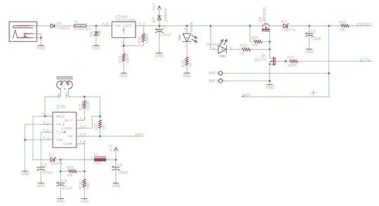
For example, here is how I would draw your boost converter (I had to stare at it for a while to figure out what it was And now I noticed you stated what it was in the question. DERP!):

The position of the main rectifier diode should make it immediately apparent now that it's a boost converter.
Also, the feedback is much easier to see.
Lastly, if you only have the battery connected to a few places, don't even use a power-port for it. Since it's only going a few places, use a wire.
Incidentally, what part is this? Now that I drew it up in my schematic library, I might as well label it properly, and maybe even use it in the future.
Other silly stuff:
C5 is 470 pF - I assume this is a ceramic? If so, don't use the schematic entity for a polarized cap. It should be two straight lines, not one straight, and one curved.
While matching the part datasheet on pin naming is almost always a good idea, there are a few edge-cases where I think being a little bit more verbose can be tremendously helpful.
If I'm doing a schematic I want to be really easy to comprehend (Or feel a bit like doing some overkill), I will actually copy the block diagram of the part into the drawing for the component in my library:
