What's the use of the teardrop shapes around some PCB pads?
What's the use of the teardrop shapes around some PCB pads?
There are primarily two reasons to use teardrops:
That being said, in professionally made PCB's teardrops are rarely needed. It's almost more of an aesthetic thing than a solution to a real problem. I've done many boards with and without teardrops and I have yet to notice a difference. In my opinion, they are more trouble than they are worth.
Electromigration is the transport of material caused by the gradual movement of the ions in a conductor due to the momentum transfer between conducting electrons and diffusing metal atoms.
– Jeff Wurz Dec 11 '15 at 09:51The teardrop is to help the drilling process. It prevents drill breakout where the trace joins the via or through-hole. Sometimes it's not necessary to do it because the manufacturer can do it for you.
Where I work, our repair department recommends we do it because it increases the strengthening of connections between pads and tracks.
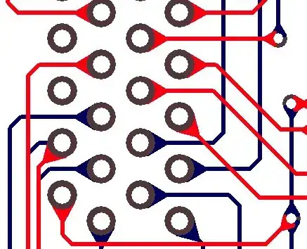
If you look at the picture the Ben Jackson posted in answer to a question about solder mask expansion, you'll see that the drilled holes can be significantly off-center from the pad centers.
In extreme cases, you could actually end up with holes that leaves no or very little annulus to make the connection to outgoing traces. The tear drop ensures that there's enough pad material left over to have a solid connection to the pad.
Perhaps the main goal is to slap a product together cheaply - they might be willing to go with a lower-precision fab, and design the board to accomodate that choice.
It might also be that there is only a small handful of parts that need extra densely placed PTH's that doesn't justify paying for higher precision fab for the other 99% of the board. The teardrop might be the "compromise" solution for those cases.
– Toybuilder Apr 19 '11 at 17:31They are mainly used on single-sided boards, to increase reliability. I often use them on my home-made PCBs.
The simple answer is for Strain Relief.
Like a plug with a thin cable, it needs a graduated support to prevent the shear forces of thermal expansion when desoldering a component or when a human interface force is involved ( eg mic jack or a heavy part on a board.)
Where you do not have strain or any thermal or mechanical stress in the application, it is unnecessary. But I have seen dozens of times when this would have prevented a track failure that was hard to see with the naked eye. One example was a $2K Mac vertical monitor with the flyback transformer on the main board... It created a micro-sheer crack impossible to see, but whenever the CRT went blank a slap to the side of the case fixed it. Which lasted for a few days, until the secretary cried.... help.. so I came to the rescue with a soldering iron. and said to myself... I wish the board designer knew about tear drop pads.
I thought it had to do with IPS-6012C for rigid board. Specifically related to section 3.4.2 Annular Ring Breakout. For example, Class 2 allow for an annular ring to break out (be missing) for 90 degrees. This is due to drill misalignment. On large vias or plated through holes, this is not likely to happen in modern fab facilities. When dealing with 10 mil finished drill holes and 20 mil pads this is much more probable. If the breakout happens on the side of the trace exiting the pad, Class 2 states that it can cut the trace down to 50um and still be acceptable. If there was a teardrop (or fillet), the misdrill would not cut into the trace.
A teardrop via make it easy to remove embedded resistors when using ECL logic. This was done by Harris Computer Systems about 1987 to make it easier to repair memory PCA's that cost upwards of $15,000 (or more) in their h1000 and h1200 systems. To remove the embedded resistor that was connected to the via all one needed was a pin vice and then drill a hole at the point of the teardrop. Then add a wire to a spare embedded resistor or add an external resistor. I remember building the light box to see the teardrop via.