2

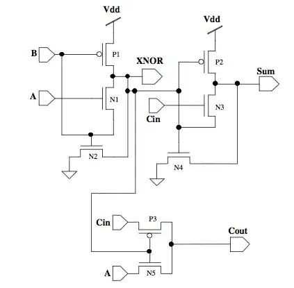
I am working on 8 Transistor full adder which is based on 3 Transistor XOR cell.enter image description here

I have studied many IEEE Papers for 8 Transistor Full adder. All have same ckt as above.But the full adder is not working properly for all inputs values. I am using Tanner EDA at 180 nm tech and 5v supply voltage for simulation purpose.

placeholder
  • 30,170
  • 10
  • 63
  • 110
GiLL
  • 133
  • 1
  • 8

1 Answers1

2

You've mixed up a few of your transistor types. Here is the actual circuit taken from Arxiv

enter image description here

Generally you want to size the PMOS width to be 2.2X wider than the NMOS but here P! and P2 should be looked at closely. P2 will fight against N3 in series with N2 and P1 will fight against N1 and the low drive form the previous gate so I'd say that P1 and P2 width for a starting estimate should be about 1.1X of the width of N1,N3 and tune from there.

P3 and N5 should follow the 2.2X rule for width ratio. Take All N's at minimum w & L.

placeholder
  • 30,170
  • 10
  • 63
  • 110
  • When B is high, N2 ties XNOR to VSS. When B is low, P1 ties XNOR to VDD. How can XNOR not equal the inverse of B? – supercat Aug 15 '14 at 17:20
  • @supercat look closely at the source of N1, when B = 0 and A =1 P1 will fight against the driver that is driving B low. You need to size the transistors properly. – placeholder Aug 15 '14 at 18:23
  • When I see CMOS, I generally assume it's designed to avoid any static shoot-through conditions. I can see how the circuit could be made to work by balancing transistors, but it would seem very "touchy" since N2 needs to be small enough to be overpowered by a series combination of N1 and whatever drives A, but large enough that in series with N3 it will be able to overpower N4 and P2. Further, if A and C are high, anything trying to pull B high will be fought by N2 and N4, and anything trying to pull it low will be fought by P1 and P2. – supercat Aug 15 '14 at 20:11
  • @placeholder thanks for your's answer after got idea i found paper https://dl.dropboxusercontent.com/u/70183915/5%20manoj%208%20t%202011.pdf i set width of p1,p2=2.0um, width for N1,N3=5.0um, width for N2,N4=1.0um and for multiplexer section take width for p3 and N5 2um,1um respectively according to paper. Then I got this WAVEFORM Full Adder http://imgur.com/EpQwGEk My question is can it be more optimized than that for more precise waveform. and in ckt diagram substrate terminal of all transistor are unconnected whether i use vdd or ground to connect it if Low Power is main concern :) – GiLL Aug 16 '14 at 04:38
  • @placeholder please help me in one more ckt.I am Also working on 6 Transistor Full adder whose ckt diagram is http://imgur.com/BhEXSwI Circuit work fine But Problem is: it need 25k resistor at XNOR and SUM point to show all Full adder pattern correctly.Because of these resistor it consume more power as compared to 8 transistor full adder but theory say less number of transistor lesser power consumption.My question:Is vary width of transistor same as 8 Transistor full adder will it show all pattern correctly without need of resistor.If yes According to u what is right widths.I hope u help me – GiLL Aug 16 '14 at 06:34
  • paper that propose 6T Full adder is https://dl.dropboxusercontent.com/u/70183915/v1i812-libre.pdf – GiLL Aug 16 '14 at 06:35
  • If you are adding in resistors, stop right there. Resistors will add cost, reduce yield and consume huge amount of area vs. a transistor solution. And I haven't even started talking about parasitic effects. – placeholder Aug 16 '14 at 07:12
  • @placeholder is there is any alternative way? to have all full adder pattern correctly without use of resistor. – GiLL Aug 16 '14 at 11:29
  • @GILL I'm not sure what you are asking. There are many ways, and you seem to be researching them 8 T , 6T etc. In general if you are building an IC you try to avoid resistors if at all possible. – placeholder Aug 16 '14 at 17:28