Yes, it's possible to damage the chip by driving it from a low impedance source when Vdd is 0.
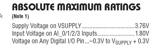
As you read from the datasheet, the absolute maximum input voltage is Vsupply -0.3. So if Vsupply is 0, you should not apply more than +/- 300mV to any input.
As well as possible damage to the particular I/O pin's protection network, if you apply power when there is an input being driven from a low impedance source, it can cause latchup, which will either short the power supply to a low voltage or destroy the chip (maybe both).
To isolate the two devices, you could use a voltage translator such as the 74AVC1T45, which goes high impedance if either Vdd is 0.
The protection network is something like a small diode between the input and Vsupply (and something similar to GND) and usually some series resistance, either of which can be damaged if you drive too much current through the input. If you drive the input to (say) 3.3V, current will flow out of the Vsupply pin and into whatever else is connected externally. At a minimum this is a big load on whatever is driving the chip even if it does not immediately cause damage.
Latchup (as described in detail in the link above) is an effect caused by the parasitic SCR structure inherent in most CMOS ICs. If a low-power chip is getting very hot to the touch, it's probably latchup.