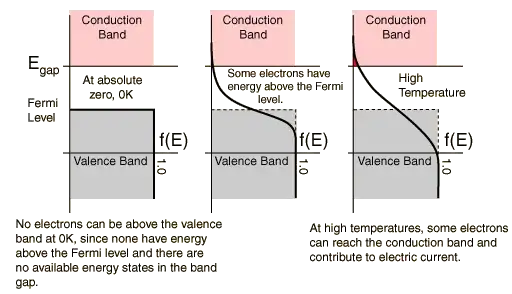
As we know, at $0 \, \rm $K, the Fermi level is the highest occupied energy state. So the top of the valence band of the intrinsic semiconductor should be the Fermi level at $0$ K. But mathematically, we get that it lies exactly at the middle of the conduction and valence band at $0$ K. Please explain what I am missing here.
3 Answers
This type of question comes up periodically, and it comes down to what exactly you are looking for (terms are often abused in this context) and how exactly you define things. The latter is “important” because there are multiple definitions of relevant terms that produce the same result at nonzero temperature but different results at zero temperature. For that reason, I wouldn’t worry about the zero temperature case, and if you insist, use a definition that is compatible with the nonzero case in the limit where temperature goes to zero.
For example, see Fermi level and chemical potential in doped and pure semiconductors and Is Fermi level located above or below donor levels in n-type semiconductor?
- 4,375
The confusion here is between Fermi energy/Fermi surface and Fermi level. Fermi energy is indeed the energy up to which the states are occupied at zero temperature, while Fermi level is the chemical potential - the parameter that enters the Fermi distribution function.
In the context of metals, at zero temperature electrons fill all the levels below the Fermi energy, which in this case is also the Fermi level. At non-zero temperature the Fermi function step becomes smooth, as electrons are transferred from just below the Fermi level to just above it.
However, in semiconductor, non-zero temperature states are obtained by transferring electrons from the top of the valence band to the bottom of the conduction band - placing the Fermi level symmetrically makes more sense (and mathematically it comes out this way because of the electron-hole symmetry - transferring electron from a valence to conduction band is like transferring an empty space from conduction to valence band, as the Fermi function is symmetric about its parameter (it is actually a hyperbolic tangent function.))
- 68,984
The Fermi level is a consequence of the Pauli exclusion principle which states that no two electrons can have the same energy state. At 0K. the electrons in the semiconductor occupy a range of energies in the ground state in order to satisfy Pauli principle and do not take on a single value. The analogy is a sea of electrons around the ground state and the Fermi level is the top of sea. No electrons are above the Fermi level. In an intrinsic semiconductor where n=p, the Fermi level is pinned at mid gap.
- 2,595
