The inductance can be calculated, but it is first necessary to look at the behavior at very fast timescales of a ns or so. Clearly the two faces of the strip form a transmission line and so, at short timescales, the resistor appears as two transmission lines in parallel. At short timescales, each line will look like a resistor of value equal to the characteristic impedance, Z, of the line. So at short time scales, this device looks like a resistor of value Z/2. But for typical construction of such a resistor with loop diameter of say 30 mm, this initial behavior will be gone in a ns or so, and then the resistance will be set by the resistivity, width and thickness and length of the conductive strips. I’m sure that when the inventor claims “no inductance”, then he means on time scales of more than a ns, after which the input to the device no longer looks like the input to a transmission line.
OK, so how might we calculate the inductance, valid for time scales greater than the transit time around the loop?
Referring to Fig1, which is a plan view, we see 2 identical loops in parallel, colored black and green, with the twist at the bottom of the sketch, near point P. The loops are identical, but the current travels in different directions around the loops. Thus the magnetic fields (almost) cancel, and the device looks (almost) non-inductive. One description is that the resistor is two anti-phased inductors wired in parallel, with a coupling coefficient almost equal to one, so that nearly all of the flux created by one coil passes through through the other. That’s fine as a qualitative description, but I asked how the inductance could be calculated. Perhaps there are a number of ways, but I offer the following.
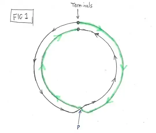
Refer to point P on the Fig 1, where the inner and outer conductors “cross over” due to the twist. It is assumed that the length of twisted section is small compared to the overall length of the loop. Symmetry tells us that this point, on both conductors, is always at a potential equal to half of the voltage applied to the resistor. As P is always at the same voltage (half of applied voltage) on both conductors, then it follows that we could electrically connect the two loops together at this point, and this would have no effect on the operation of the circuit.
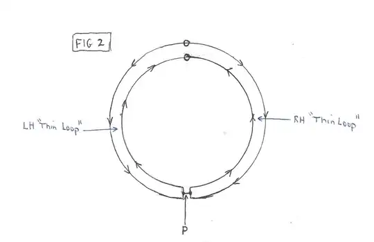
Fig 2 shows the equivalent circuit thus created by connecting the loops together at this point. Note that the small, horizontal link at P in Fig2 is not actually doing anything. From symmetry considerations there will be no current through this link – if there was then in which direction would the current be? And as there is no current through this link, then it can be removed without changing the operation of the circuit.
In Fig 3, this small link has thus been removed. Also, the two long, thin loops have been straightened, which will also not affect the operation of the circuit, noting that the Bfield from these thin loops is very localized in the small gap between conductors, so the field from one does not interfere with the other (or with anything else nearby), so we are free to straighten or bend these loops as we choose without affecting the operation of the circuit.
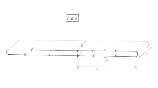
So we end up with the equivalent circuit of Fig3, where the resistor input terminals are still connected to two loops in parallel, but now the loops in question are long and very thin, magnetically separate, and their inductance is easily calculated with application of Ampere’s Law.
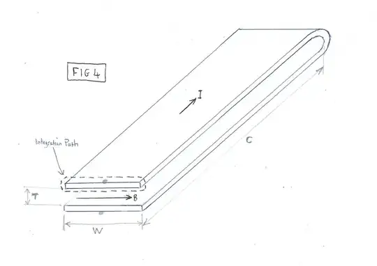
Fig 4 illustrates the method for finding the inductance of one of these long, thin loops. Provided the strip width and length are large compared to the separation, then to a good approximation, the Bfield is strong and uniform between the conductors, and zero everywhere else. Amperes Law states :-
$$\oint B.dl = \mu_0 I$$
Where Integral $\oint B.dl$ is a line integral is around a closed loop, $I$ is the current passing through the loop, and $\mu_0$ is magnetic permeability of free space
The line integral is easily calculated, because there is a constant field B along the bottom of the rectangular integration path, the vertical legs of the path are of negligible length, and the field is zero along the top of the path.
$$\oint B.dl = \mu_0 I$$
$$BW = \mu_0 I$$
$$B=\frac{\mu_0 I}{W}$$
Total flux through the loop = $\Phi = BA = BTC = \frac{\mu_0 ITC}{W}$
where
$T$ is conductor separation and $C$ is loop length, in this case half of the total Mobius loop length.
Finally,
$L \text{(Henry)} = \frac{\Phi}{I}$ (can be found in any textbook)
$L = \frac{\mu_0 TC}{W}$ (for one loop)
$$\bf L_\text{mobius} = \frac{\mu_0 TC}{(2W)}$$ (because there are 2 identical loops in parallel)
How beautifully simple. So to minimize the inductance, you need small strip separation, small length of Mobius loop, and a wide strip. The Bfield from these narrow loops is very localized in the small gap between conductors, so the field from one does not interfere with the other (or with anything else nearby) and the Mobius loop can thus be bent into an ellipse or other shape without affecting the inductance seen between the terminals.
OK. So the formula shows that the inductance is not inherently zero as claimed, but just how small will it be for typical construction? Assume the following dimensions.
$T = 0.05 mm = 0.05\times 10^{-3} m$
$C = 47 mm = 0.047 m$ (corresponds to D=30mm)
$W = 10 mm = 0.01 m$
$\mu_0 = 1.26\times 10^{-6}$ (for free space, as no magnetic materials are present)
.
$L = uTC/(2W)$
$L = 1.48\times 10^{-10}$ Henry = 0.148 nH
That is a very low inductance to be sure, ideal for fast current sensing. To exploit such low inductance will require Kelvin sense terminals (4-wire resistor) which is easily accomplished, otherwise the inductance of the lead-in wires will far exceed that of the resistor itself. To put the value of 0.15 nH in perspective, the package inductance of the mosfet source connection on a TO220 power semiconductor package is about 5 nH, measured 6 mm from the die, so 0.15 nH is an absurdly small value of inductance for an electronic component.
I will later add more text to show a better method of constructing low-inductance resistors, that I have been using for decades with good results.