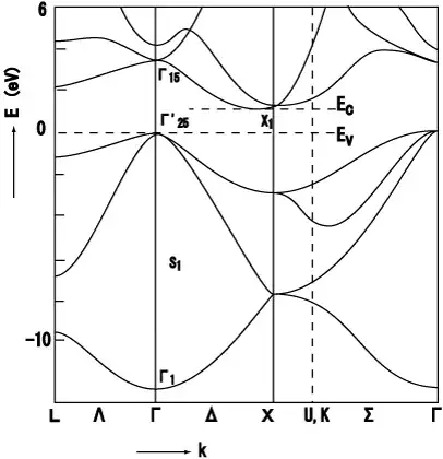
(1) The diagram shows which electron reciprocal lattice vectors (i.e. momenta) correspond to which energies. These are the eigenvalues of the lattice. A (Bloch) electron can only have an energy+momentum that falls on one of the curves (but not the vertical/dashed lines; those are just guides for the eye). You'll notice that between 0 eV and ~1 eV, there are NO curves for any momentum. This is the definition of a band gap, i.e. there are no electron states anywhere in the (0 to ~1) eV range.
(2) I mentioned above what a band gap is, but for it to practically function as a gap, the states below it have to be (mostly) filled, and the states above it must be (mostly) empty. For this, you look where the zero energy is, which is the location of the Fermi surface. So if the crystal is undoped and at zero temperature, all the states below 0 eV will be full of electrons (all these states together are the "valence band"), and all the states above 0 eV will be empty of electrons (together, the "conduction band"). Since 0 eV here corresponds to the top of the valence band (energy $E_v$), then the band gap is important. You can see this will be a semiconductor because the bottom of the conduction band (energy $E_c$) is only ~1 eV above $E_v$. Any band gap $E_g=E_c-E_v$ less than around 3 eV we call a "semiconductor."
So how do you read this? The different labels on the independent axis ($\Gamma$, X, etc.) correspond to different "momenta of high symmetry". This will make more sense if you look at an image of the reciprocal lattice unit cell. But a lot of the details don't really matter. Really, you want to focus on the states around the gap, as these are where most lowish-energy processes occur (~room temp conductivity, visible/IR light interaction, etc.). Use this to understand what these band-edge states are like and to think about what would be needed for an electron to move from one state to another. Interactions must conserve energy and momentum. Some things you can glean, for example:
(a) Curvature tells you about effective mass (more curvature near $E_v$ and $E_c$ means low mass and potentially high electron/hole mobility). E.g. the two curves at $\Gamma$ around $E_v$ are the "light hole" and "heavy hole" bands.
(b) The top of the valence band ($\Gamma$) is not at the same momentum as the bottom of the conduction band (near X). This makes the band gap "indirect", which means for an electron to transition from $E_c$ to $E_v$, it needs to lose a bunch of momentum (more than light will give, for example). This is why you can't easily make a laser out of Si: light can give you the energy, but not the momentum, to transition from $E_c$ to $E_v$.
(3) First of all, you don't mean one atom (which has discrete energy levels and no $k$-space), you mean a simple crystal (perhaps 1D chain?) of one atomic species. But the number of atomic species doesn't matter for whether there's a band gap. Case in point, your example band structure is for a crystal with just one atomic species (Si). There is very little intuitive about what crystal lattice will result in what band structure; you just have to crank through the complex calculations. For a little more on this: Why is there more than one band?, What's the difference between transparent and opaque materials at the atomic level?