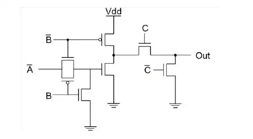
I have this circuit for which I have to find the truth table for all imputs whether they are logic 1 (VDD), logic 0 (GROUND) or X unknown. But I am having trouble understanding what I am supposed to do to find the OUTPUT when the imput is unknown..
I have this circuit for which I have to find the truth table for all imputs whether they are logic 1 (VDD), logic 0 (GROUND) or X unknown. But I am having trouble understanding what I am supposed to do to find the OUTPUT when the imput is unknown..
You simply need to break it down moving from the output to the input.
C = 1: Out = floating (i.e. X) unless the node on the inverter is driven low.
C= 0: Out = 0 unless the PMOS on the inverter has strength enough to drive the NMOS (with /C on it), but since this is driven through another NMOS (with C on it) it's hard to tell.
This question as posed needs transistor sizing information to be of any value at all.
The way to approach this problem is to tackle ON/OFF states of devices for all combinations of boolean inputs A, B and C. You can label the transmission gate, PMOS, NMOS transistors. Make a truth table with A,B,C as inputs and outputs as state(ON/OFF) of individual devices plus Out. You will find that Out is either connected to Vdd (HIGH) or ground (Vss i.e. Low) and is never floating(open circuit or High-impedance).
Out is High only for two combinations: A=0, B=1, C=1; A=1, B=1, C=1. For all other combinations, Out is always connected to ground(Vss)