There is a circuit based on TTL( transistor transistor logic I think) . The signals at points A B C D are described. I am new with this TTL, could you help me decompose this united circuit into the logic components which it consists from? Thanks.


It seems to be a simple inverter.
Assuming no other connections, resistors and supply as shown, we can simplify the circuit as so:
simulate this circuit – Schematic created using CircuitLab
which has a DC transfer function from V1 (A) to D,

give or take the setting of your R13, here set all the way towards C.
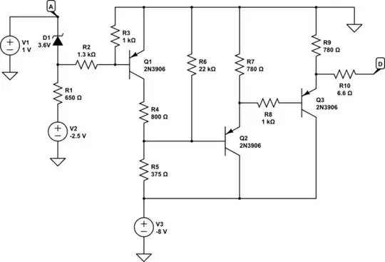
It's more or less an emitter follower-buffered negative-voltage (PNP type) RTL inverter, with level shift at the input.
The Darlington follower (Q2 into Q3) doesn't seem very useful, but without knowledge of application and ratings, that's neither here nor there.
V_CONis, and what J11-J14 are or what might be attached to them? – Tim Williams Mar 30 '24 at 10:38