1

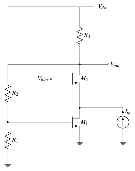
Here is the circuit from YouTube:

enter image description here

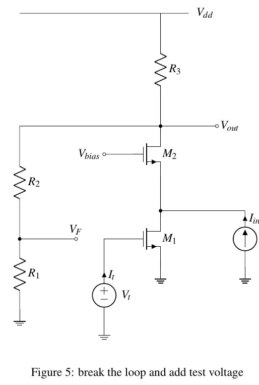
In order to determine the feedback, we have to break the loop at the gate of M1.

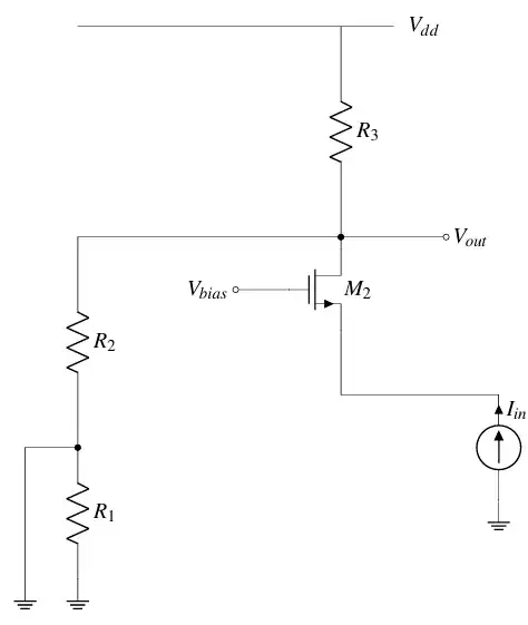
Assume A is \$\infty\$, so \$V_{GS}\$ of M1 is 0. As we know the \$V_S\$ of M1 is grounded, we have \$V_S = V_G = 0\$. And that's why the gate of M1 is grounded.

enter image description here

$$\frac{V_{out}} {I_{in}} = R_2 \parallel R_3$$

The following is how I break the loop and add test voltage.

enter image description here

$$Loop \hspace{1mm} Gain = L = \frac{V_F} {V_t} = g_{m1} \bigr(R_3 \parallel (R_1 + R_2)\bigr) \frac{R_1} {R_1 + R_2}$$
kile
  • 798
  • 2
  • 11
  • Why do you call it a current-voltage feedback circuit? It's a potential divider and the attenuation it provides is the feedback factor. – Andy aka Mar 24 '24 at 10:05
  • @Andyaka What's the $\beta$ according to you? – kile Mar 24 '24 at 10:38
  • $\dfrac{R_1}{R_1+R_2}$ and, you don't need to break any loops to see this. – Andy aka Mar 24 '24 at 10:43
  • @Andyaka Nope, check https://youtu.be/L-fihvU3VC8?list=PLc7Gz02Znph-c2-ssFpRrzYwbzplXfXUT&t=2452 – kile Mar 24 '24 at 11:18
  • Sorry but youtube is not a technical authority that can be trusted. There are many sources that agree with me: https://www.google.com/search?sca_esv=2e0a38931ff166af&rlz=1C1_____en-gbGB1078GB1079&sxsrf=ACQVn09oku885gRJdA3Ap1HBTGkuovFCKg:1711286165443&q=amplifier+feedback+coefficient&tbm=isch&source=lnms&prmd=ivnbmtz&sa=X&ved=2ahUKEwi28v_f_YyFAxV7QkEAHbMiBr0Q0pQJegQICRAB&biw=1680&bih=901&dpr=1#imgrc=PTe5_wHtMSa1AM – Andy aka Mar 24 '24 at 13:14
  • @kile You should include M1 in the feedback network. – internet Mar 24 '24 at 15:00
  • @internet What does the feedback network look like? – kile Mar 24 '24 at 15:09
  • @internet Is this feedback network the same as https://i.stack.imgur.com/Kc1zL.png – kile Mar 24 '24 at 15:41
  • @kile yes because they're the same circuit – internet Mar 24 '24 at 15:47
  • I’m voting to close this question because academic questions need an attempt at a solution – Voltage Spike Mar 25 '24 at 17:07
  • @VoltageSpike I have tried to solve this with my way. But they said it's not correct. The following is what I have tried.

    Assume A is $\infty$, so $V_{GS}$ of M1 is 0. As we know the $V_S$ of M1 is grounded, we have $V_S = V_G = 0$. And that's why the gate of M1 is grounded.

    – kile Mar 25 '24 at 18:47
  • @VoltageSpike See my updates on my question – kile Mar 25 '24 at 22:22
  • @internet Do I add my test voltage correctly? https://electronics.stackexchange.com/questions/707531/how-can-i-calculate-loop-gain-when-considering-loading-effect-in-voltage-current – kile Mar 27 '24 at 08:10

2 Answers2

3

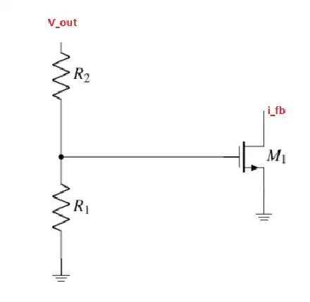
The feedback network includes R1, R2, and the transistor M1. The feedback factor \$\beta\$ is calculated as follows:

\$\beta = \frac{i_{fb}}{V_{out}} = g_{m1}\cdot\frac{R1}{R1 + R2}\$

enter image description here

internet
  • 544
  • 1
  • 3
  • 13
  • I think the trickiest thing is how to find the feedback network. Can you explain how you find this feedback network? – kile Mar 25 '24 at 06:53
  • @kile - the above consideration is correct (see my detailed answer). – LvW Mar 25 '24 at 08:59
  • @kile If you compare the circuit with this diagram here, you can identify different parts of the feedback network. Also, check the LvW answer. – internet Mar 25 '24 at 16:21
  • @internet I draw a a schematic on how I break the loop. Can you see my updates on the question? Do I break the loop correctly? – kile Mar 25 '24 at 22:24
  • @kile Yes, you can break the loop like that but you make a mistake in your calculate of LG. – internet Mar 26 '24 at 02:47
  • @internet Do we have to consider loading effect? – kile Mar 26 '24 at 08:24
  • @kile no, you don't need to add loading effect in this case. – internet Mar 26 '24 at 08:30
2

Here comes my explanation of the shown circuit:

1.) The input of the amplifier (common gate configuration with a current input) is the source node of M2.

2.) Therefore, the feedback signal (in form of a current) is superimposed at this node with the signal current. That means: Transistor M1 is part of the feedback path. It is its purpose to convert the feedback voltage (at the gate of M1) into a current.

3.) Opening the feedback loop at the gate of M1 and injecting a test voltage Vt,in, we get the loop gain expression:

Loop gain LG=Vt,out/Vt,in with

id1=gm1*Vt,in and

Vt,out=[R1/(R1+R2)] * id2 * R3||(R1+R2)

Loop gain LG=Vt,out/Vt,in=[R1/(R1+R2)] * (id2/id1) * gm1 * R3||(R1+R2)

Because of id2=id1 we can simplify:

LG=[R1/(R1+R2)] * gm1 * R3||(R1+R2)

The gain of the open loop is

Aol=Vout/i,in=R3||(R1+R2)**

Therefore the feedback "factor" is beta=LG/Aol:

beta=[R1/(R1+R2)] * gm1.

LvW
  • 26,610
  • 3
  • 23
  • 56