I don't know why you say current \$I_3\$ through R3 is \$I_3=\frac{\Delta V_{GS}}{R_3}\$. I would say that \$\Delta V_{GS}\$ is the potential difference between the gates, and is not the voltage across R3. That seems to be the mistake you made, but I had trouble following your derivation, because I have no idea what \$V_{OUT1}\$ and \$V_{OUT2}\$ are.
In any case, my approach is not like yours. Start with some labels:
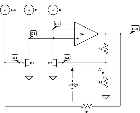
simulate this circuit – Schematic created using CircuitLab
Not that it's relevant, in case my previous statement wasn't clear:
$$ I_3 = \frac{V_{G2}}{R_3} $$
Here \$V_{G2}\$ is the absolute potential at the gate of Q2, w.r.t 0V, and is not directly related to \$\Delta V_{GS}\$.
Due to negative feedback:
$$ V_{D1} = V_{D2} $$
Therefore, both JFETs are passing the same current, and have equal \$V_{DS}\$, which is the principle on which this design depends. The two transistors are biased to produce identical drain conditions, which is why we are able to say that the difference between absolute gate potentials will be the difference between the two transistors' respective \$V_{GS}\$:
$$
\begin{aligned}
\Delta V_{GS} &= V_{GS1} - V_{GS2} \\ \\
&= (V_{G1}-0V) - (V_{G2}-0V) \\ \\
&= V_{G1}-V_{G2}
\end{aligned}
$$
Gate-channel junctions are reverse biased, so gate currents are negligible, and need not be considered when calculating gate potentials:
$$ V_{G1} = V_{OUT} + I_{PTAT}R_1 $$
R2 and R3 are a potential divider between OUT and ground:
$$ V_{G2} = V_{OUT}\frac{R_3}{R_2+R_3} $$
Combining those last three equations:
$$
\begin{aligned}
V_{G1} - V_{G2} &= (V_{OUT} + I_{PTAT}R_1) - V_{OUT}\frac{R_3}{R_2+R_3} \\ \\
\Delta V_{GS} &= I_{PTAT}R_1 + V_{OUT}\left(1 - \frac{R_3}{R_2+R_3} \right) \\ \\
&= I_{PTAT}R_1 + V_{OUT}\frac{R_2}{R_2+R_3} \\ \\
V_{OUT} &= \frac{\Delta V_{GS} - I_{PTAT}R_1}{\left(\frac{R_2}{R_2+R_3}\right)} \\ \\
&= (\Delta V_{GS} - I_{PTAT}R_1)\frac{R_2+R_3}{R_2} \\ \\
&= (\Delta V_{GS} - I_{PTAT}R_1)\left( 1 + \frac{R_3}{R_2} \right) \\ \\
\end{aligned}
$$
Update
There's an error in my circuit above. I've labelled nodes D1 and D2 representing drains, but actually the JFETs are source followers. It would have been better to label them S1 and S2. That doesn't change the behaviour at all, because JFETs are typically symmetrical, and you can swap drain and source without changing behaviour, it's just the labels that are misleading.
A simulation using actual JFETs might have trouble solving for the DC operating point, because the op-amp will initially have 0V output, effectively forward-biasing the JFET junctions. That can be addressed by connecting the drains to a negative potential in the simulation, which I'll try in a moment.
For now, though, I want to simulate behaviour with the following in mind:
Those source followers will merely subtract the transistor's \$V_{GS(OFF)}\$. That is, if \$V_{GS(OFF)}=2V\$, then \$V_S = V_G - 2V\$.
A source follower's voltage gain is \$\frac{\Delta V_S}{\Delta V_G}\approx+1\$.
The constant current \$I_{PTAT}\$ through R1 will similarly just apply some fixed offset voltage to \$V_{OUT}\$.
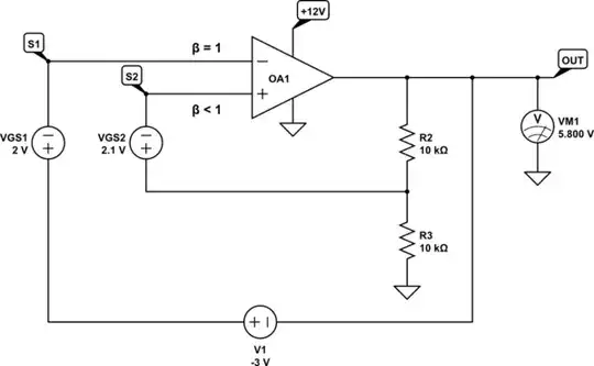
simulate this circuit
In this scenario, \$\Delta V_{GS}\$ is:
$$ \Delta V_{GS} = V_{GS1} - V_{GS2} = -0.1V $$
Also:
$$ I_{PTAT}R_1 = V_1 = -3V $$
$$ 1+\frac{R_3}{R_2} = 2 $$
Therefore:
$$
\begin{aligned}
V_{OUT} &= (\Delta V_{GS} - I_{PTAT}R_1)\left( 1 + \frac{R_3}{R_2} \right) \\ \\
&= \left[(-0.1) - (-3)\right] \times 2 \\ \\
&= +5.8V
\end{aligned}
$$
You may have noticed that I swapped the op-amp's inverting and non-inverting inputs. For this system to be stable, negative feedback should dominate. In other words, feedback factor \$\beta\$ must be larger at the inverting input. Clearly R2 and R3 produce a feedback factor \$\beta < 1\$, while for the other path \$\beta = 1\$, and so I believe the inverting input should "see" the greatest change in potential in response to a change in \$V_{OUT}\$, which corresponds to \$\beta = 1\$ in this design.
I think I'll get some flak for suggesting this, but did Horowitz and Hill get the op-amp's inputs the wrong way around here?
The other thing you might notice is that I've arranged for the offset V1 to be negative. The op-amp cannot produce negative output potentials, which it might have to do in order to properly bias Q1, if that offset were strongly positive. I don't think this is an "error" in the design, just something that isn't immediately obvious.
As I mentioned before, I think for a simulation using JFETs to work, we must somehow arrange for it to be impossible for the JFET gate-channel junctions to be forward biased. The simplest way I can think of to achieve that is to set drain potential to be much more negative than the op-amp output could ever be:
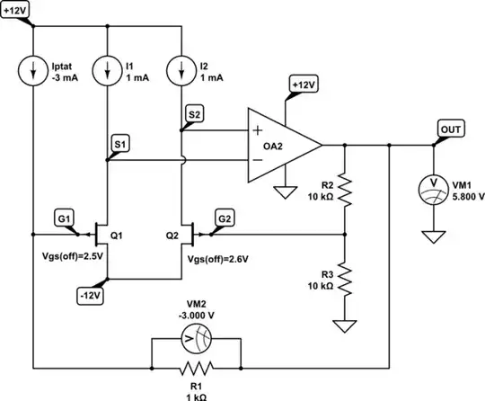
simulate this circuit
Notice that \$I_{PTAT}\$ is negative here, to place the offset to \$V_{G1}\$ in a range compatible with the op-amp's constrained output swing.
The other point to note is that I've connected drains to −12V. That might not be necessary in your simulator. CircuitLab seems to work with drains grounded, but I'm still wary of the DC operating point being ambiguous when the junctions are forward biased.
Edit: Actually, now I think of it, there's no region in the graph of \$V_S\$ vs. \$V_G\$ where the slope is negative (which could potentially cause feedback to become positive), so I think you should be fine grounding the drains of JFETS.
The hardest part about getting this circuit to work is finding values that don't cause the op-amp to saturate. Using the 2N5460 JFET, for example, which has a significant \$V_{GS(OFF)}\approx3V\$, the op-amp must produce a strongly positive output to bias Q1; remember that Q1's gate voltage is only a fraction of \$V_{OUT}\$.
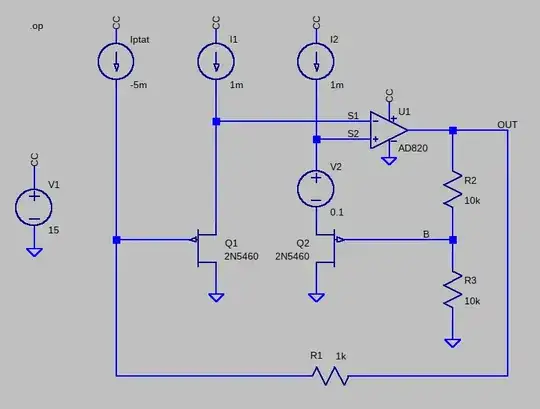
Here's an implementation in LTSpice, using the 2N5460, with values tweaked to make it work:
The .asc file from LTSpice:
Version 4
SHEET 1 880 680
WIRE -336 -32 -336 -48
WIRE -160 -32 -160 -48
WIRE 16 -32 16 -48
WIRE 144 96 144 80
WIRE -160 112 -160 48
WIRE 80 112 -160 112
WIRE 112 112 80 112
WIRE 256 128 176 128
WIRE 352 128 256 128
WIRE 16 144 16 48
WIRE 80 144 16 144
WIRE 112 144 80 144
WIRE 144 176 144 160
WIRE 16 192 16 144
WIRE 256 192 256 128
WIRE -480 224 -480 192
WIRE -160 288 -160 112
WIRE 16 288 16 272
WIRE -336 320 -336 48
WIRE -208 320 -336 320
WIRE 208 320 64 320
WIRE 256 320 256 272
WIRE 256 320 208 320
WIRE -480 336 -480 304
WIRE 256 368 256 320
WIRE -160 416 -160 384
WIRE 16 416 16 384
WIRE 256 496 256 448
WIRE -336 560 -336 320
WIRE 0 560 -336 560
WIRE 352 560 352 128
WIRE 352 560 80 560
FLAG 144 176 0
FLAG -480 336 0
FLAG -480 192 CC
FLAG 144 80 CC
FLAG 256 496 0
FLAG 352 128 OUT
FLAG 80 144 S2
FLAG 16 416 0
FLAG 80 112 S1
FLAG 208 320 B
FLAG 16 -48 CC
FLAG -160 -48 CC
FLAG -160 416 0
FLAG -336 -48 CC
SYMBOL voltage -480 208 R0
SYMATTR InstName V1
SYMATTR Value 15
SYMBOL res 240 176 R0
SYMATTR InstName R2
SYMATTR Value 10k
SYMBOL res 240 352 R0
SYMATTR InstName R3
SYMATTR Value 10k
SYMBOL pjf 64 384 R180
WINDOW 0 60 57 Left 2
WINDOW 3 60 35 Left 2
SYMATTR InstName Q2
SYMATTR Value 2N5460
SYMBOL current 16 -32 R0
WINDOW 123 0 0 Left 0
WINDOW 39 0 0 Left 0
SYMATTR InstName I2
SYMATTR Value 1m
SYMBOL pjf -208 384 M180
WINDOW 0 63 58 Left 2
WINDOW 3 62 34 Left 2
SYMATTR InstName Q1
SYMATTR Value 2N5460
SYMBOL current -160 -32 R0
WINDOW 123 0 0 Left 0
WINDOW 39 0 0 Left 0
SYMATTR InstName I1
SYMATTR Value 1m
SYMBOL current -336 -32 R0
WINDOW 123 0 0 Left 0
WINDOW 39 0 0 Left 0
SYMATTR InstName Iptat
SYMATTR Value -5m
SYMBOL res 96 544 R90
WINDOW 0 -11 80 VBottom 2
WINDOW 3 -29 37 VTop 2
SYMATTR InstName R1
SYMATTR Value 1k
SYMBOL voltage 16 176 R0
SYMATTR InstName V2
SYMATTR Value 0.1
SYMBOL OpAmps\\AD820 144 64 R0
SYMATTR InstName U1
TEXT -488 -56 Left 2 !.op
DC operating point results:
V(out):      10.2009     voltage
V(b):        5.10044     voltage
V(s2):       2.79732     voltage
V(s1):       2.79728     voltage
I(Iptat):   -0.005   device_current
I(I1):       0.001   device_current
I(I2):       0.001   device_current
For this circuit:
$$ \Delta V_{GS} = 0.1V $$
$$ I_{PTAT}R_1 = -5V $$
$$ 1+\frac{R_3}{R_2} = 2 $$
$$
\begin{aligned}
V_{OUT} &= (\Delta V_{GS} - I_{PTAT}R_1)\left( 1 + \frac{R_3}{R_2} \right) \\ \\
&= \left[(0.1) - (-5)\right] \times 2 \\ \\
&= +10.2V
\end{aligned}
$$
As you can see, \$V_{OUT}\$ gets very high. I recommend trying to modify the parameters, one by one, to see how easy it is to cause the op-amp to to leave its comfort zone, and why it can be challenging to find a confiuration that works.


