2

I’d welcome some advice on a hobbyist peripheral interface design.

This must use 74-series logic and have the lowest package count.

There is a notional CPU which is not shown in the sketch below. It is separate from the peripheral interface and connected to it via an external cable that has 8 data lines (plus ground), through which it can send a series of bytes/logic values. There's no specific software transfer protocol yet, this will be dictated by the needs of the interface design being discussed in this post.

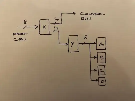
The peripheral interface will have an 8-bit latch, [X] on the sketch below, like a 74HC373, that receives data from the CPU. There is a dedicated latch enable line under CPU control not shown in the sketch, but this cannot be repurposed - its sole role is to ensure that data is supplied to X correctly.

The 8-bit values latched into [X] are stable, until the next byte is sent. These bytes are sent by control software running on the CPU, which itself is clocked at around 1 Mhz.

I can’t add any more data lines to the cable, I only have 8 to work with.

From this single port, I need to populate four other HC373 type latches or registers [A, B, C & D] with specific data. Software can be written to get the CPU to send any required combination of 8-bit values, in order to achieve this.

The current thinking is to use 4 bits of [X] for nibbles of data, and the other 4 as control bits. Two address bits to select [A], [B], [C] or [D] and a third control bit as a latch enable or clock line for them.

Next, that [X] connects to a dual 4-bit latch (perhaps a 74HC873) [Y], that recreates an 8-bit data byte from each pair of 4-bit nibbles using the fourth control bit (Hi/Lo). This then connects to one of [A], [B], C] & [D] depending on the control bits (00, 01, 10 or 11), and the data is latched/clocked.

In summary, the data values that end up in [A] thru [D] are envisaged as being sent by the CPU as 8 nibbles. Bits 0..3 at [X]'s output are those nibbles, and bits 0..4 provide the control bits that orchestrate this re-assembling of the data values.

I’ve got brain fog, and can’t come up with a circuit design despite numerous scribbles. It feels like there needs to be an additional control bit to latch data into the relevant 4-bit nibble latch, but there's probably a smart way to get around this.

Can anyone suggest a simple solution please?
enter image description here

David00
  • 183
  • 9
  • Comments have been moved to chat; please do not continue the discussion here. Before posting a comment below this one, please review the purposes of comments. Comments that do not request clarification or suggest improvements usually belong as an answer, on [meta], or in [chat]. Comments continuing discussion may be removed. – Voltage Spike Jan 31 '24 at 00:22

3 Answers3

3

From what you've described so far, you could use the following...

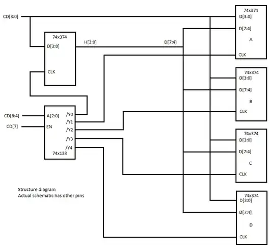
The scheme is to write data bytes for 8-bit registers A, B, C and D as two nybbles (Most Significant Nybble, Least Significant Nybble). The MSN gets written into a holding register, H, then it and the LSN get written simultaneously to the 8-bit register.

This needs 6 ICs: 4x 74x374 8-bit D-type Flip-Flop (DFF) IC; 1x 74x138 IC; 1x holding register IC.

The 8-bit cable data, CD[7:0], is allocated as follows:

  CD[3:0]   Write data nybble
  CD[6:4]   Device address
  CD[ 7 ]   Load enable

CD[3:0] go to:

  • 'D[3:0]' of 4-bit holding register H, which has outputs H[3:0].
  • 'D[3:0]' of 8-bit registers A, B, C and D.

H[3:0] go to the D[7:4] of 8-bit registers A, B, C and D.

CD[6:4] go to the A[2:0] inputs of a 74x138 decoder.

CD[7] goes to the active-high 74x138 ENable input G2.

The 74x138 outputs are connected as follows:

  • /Y0 goes to clock/latch of H.
  • /Y1 goes to clock/latch of A.
  • /Y2 goes to clock/latch of B.
  • /Y3 goes to clock/latch of C.
  • /Y4 goes to clock/latch of D.

The procedure to load A, B, C or D with data byte xxxxyyyy is:

  Load CD[7:0] with 0000xxxx   ;Set up holding latch address and the write data
  Load CD[7:0] with 1000xxxx   ;All stable, take H`'s CP LOW
  Load CD[7:0] with 0000xxxx   ;Keep stable while taking H's CP HIGH to load

Load CD[7:0] with 0aaayyyy ;Set up device address and the write data Load CD[7:0] with 1aaayyyy ;All stable so take register's CP LOW Load CD[7:0] with 0aaayyyy ;Keep stable while taking register's CP HIGH to load

where aaa is: 001 for A, to 100 for D.

The circuit structure diagram below illustrates this. H is shown as another 74x374 but could be a 4-bit register in a smaller IC.

enter image description here

TonyM
  • 22,898
  • 4
  • 39
  • 64
  • Thanks for the suggestion. Doesn’t this load 4 bits of data into one of the 4 data end-points [A] thru [D]? But each of them is 8-bits wide. I’m struggling with the nibbles to byte assembly at Y, as I don’t have enough derived control lines. – David00 Jan 30 '24 at 23:37
  • @David00, I must have misunderstood your question, then. So you could pass data up the 8 wires in nybbles. And you want to load data into 4x 8-bit latch. Are both those right? – TonyM Jan 30 '24 at 23:44
  • Yes. I know that every byte sent from the CPU must comprise some control bits and some data bits. The end goal is to encode data in the sent byte so as to end up with four 8-bit data bytes into [A] thru [D]. I’d considering sending nibbles, and reassembling them at Y using a fourth hi/lo control line/bit in the sent byte. But I think I need an extra control bit as a clock/enable for Y. I’m wondering if 1 bit in the sent byte could define/change the split between data and control bits to get around this. – David00 Jan 31 '24 at 00:03
  • @David00, revised, this should do what you want. – TonyM Jan 31 '24 at 01:06
  • Thanks, will need to look at properly in the morning. – David00 Jan 31 '24 at 01:18
  • 1
    This is a an elegant solution. I've realised that by focusing on 8 bit regs, I didn't think about pre-loading 4 bits into a H type reg. The fog has cleared. Thank you for your patience and guidance throughout, much appreciated. – David00 Jan 31 '24 at 20:20
  • @David00, glad you think so and thanks for showing that with an upvote :-) – TonyM Feb 01 '24 at 00:15
1

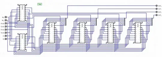
Thanks for the discussion. In keeping with your idea of using 74373. But the following uses the edge-type 74374 (possibly fewer update clocks required -- especially if you can skew the clock slightly -- but check just in case):

enter image description here

The protocol would be the following:

  • Clock \$W_{_\text{HI}}\$ with \$P_3\dots P_0=0\$ and \$D_1 D_0\$ set to the upper 2 bits of the data to be written.
  • Clock \$W_{_\text{LO}}\$ with \$D_5\dots D_0\$ set to the lower 6 bits of the data to be written.
  • Clock \$W_{_\text{HI}}\$, with \$D_1 D_0\$ still set to the upper 2 bits of the data to be written, but now also clocking one of \$P_3\dots P_0\$ depending on the desired output port to update.

For example, to write 0xA5 to \$OUT_2\$ use: 0x82, 0x65, 0x92, 0x00. Or, to write 0xA5 to \$OUT_2\$ and 0xE7 to \$OUT_0\$ use: 0x82, 0x65, 0x92, 0x83, 0x67, 0x87, 0x00. (That last 0x00 is just to put everything back to rest.)

Here's a longer example showing the above two port writes plus another two so that all four port outputs are set:

enter image description here

That's it. Every three writes updates a port. Not too shabby.

As I said, I'd probably go with 74374's instead of 74373's and add some clock skew. The transparent mode otherwise requires an extra cycle, which I'd rather avoid.

periblepsis
  • 8,575
  • 1
  • 4
  • 18
  • 1
    This is a very clever design. I want to thank you for all of your suggestions. You may not recall that you helped me with another question some time ago. I'm really grateful to you for taking the time to think this through. – David00 Jan 31 '24 at 20:34
  • @David00 I don't specifically recall. But hopefully I was nice about it. ;) So are you going to give this a try? (By the way, I cannot tell you how much suffering I went through to learn this stuff back in 1973/1974, designing my own CPU then. I was totally ignorant to start -- suffered mightily for a year -- and finally got things working. Once that kind of thing deepens into your soul painfully like that, it doesn't go away in time. It sticks.) – periblepsis Jan 31 '24 at 20:38
  • @Periblesis: I'm a slightly later vintage. I was building circuits and kits in the late 70s/early 80s as a teenager. Then worked on BIOS & DOS dev in the late 80s for several years. I've looked through your design. I can see how it works, section by section, but wouldn't be able to envisage it hence why I needed help. This design is part of a larger one - but I will try it out. – David00 Jan 31 '24 at 21:01
  • @David00 Sounds similar to my experiences. I worked on Unix v6 (1978) where I learned C. I also worked on Phoenix BIOS team at Intel for a while -- during transition from 32-bit to 64-bit. Did a lot of DOS dev in assembly in the early 1980's, until C arrived mid-1980's and later where I worked mixed lang for a while. Mostly since mid 1980's doing embedded instrumentation, working on writable CD optics design, on-contact temp meas., etc. Let me know if it works as I think it will. (If I had the parts handy (I don't) I'd just wire it up and make sure.) – periblepsis Jan 31 '24 at 21:06
  • Small world. I was an FAE for Phoenix Technologies, covering PC OEMs in Europe in the 90s. But haven’t worked in engineering for over 28 years. Just getting back into it for fun :-) Thanks once again. – David00 Jan 31 '24 at 23:49
1

I have not worked out all the details, but one approach might be divide bytes into two types, distinguished by, say their most significant bit. One type of byte will be a control byte, the other a data byte. Each data byte has 7 significant bits. A johnson/ring counter is used to address/enable, in sequence, 5 8-bit latches. When each data byte is received, 7 bits are fed into one of the 5 8-bit latches. One of the latches, say the 5th, provides the missing bit for each of the other latches. The missing bits don't need to actually be fed into the latch. One can merely use seven bits from one latch, and one bit from another latch.

Control bytes could 1) reset the johnson counter, enable or tri-state outputs, or other tasks that might be appropriate.

Math Keeps Me Busy
  • 23,260
  • 4
  • 21
  • 75
  • Thank you for this suggestion. I'd envisaged this as an option, but hadn't been able to think it through the way you have. I've had two good answers already, but have learnt something new from your design approach. – David00 Jan 31 '24 at 20:37