Can anyone explain how this topology works and/or point me to any literature where it is discussed?

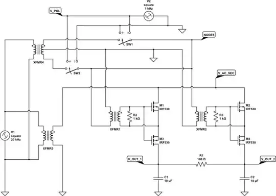
I've found Microchip's application notes on single stage interleaved flybacks with SCR or MOSFET unfolding bridges and have a pretty good understanding of those. My best guess is this is also a single stage inverter (boost and dc to ac inversion is happening with the full bridge and transformer). I assume a full bridge is used for good transformer utilization while keeping device voltage ratings low. I'm having trouble though understanding how what I assume would be chopped up AC gets coupled to the grid through the dual MOSFET and capacitor bridge.
This paper shows something similar (full dual switch bridge instead of caps on bottom) in section III C but I haven't tracked down the references where it is discussed (yet) to see if they could fill in the gaps for me.
Image created by me based off of a tear down of a broken unit. Note there are some x caps and common mode chokes between the output dual switch/cap circuit and ac connection not detailed here which I assume isn't meaningful for the topology and only for EMC.
Lots of assumptions.
Edit: Including annotated photo of PCB. No components on bottom side.
