1

The following is the logic diagram of a single pole double throw analog switch that I am trying to use.

Specifically what I am wondering is if it connects one of nY or nZ to ground when nE is low.

But I also have no real clue on how to interpret this in general. Specifically the center connections to the mosfets have me confused as I have never seen that before and I do not know which terms to search for to find out what they are doing.

For context, the diagram is from this chip: https://assets.nexperia.com/documents/data-sheet/74LV4066.pdf
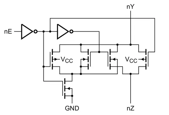
Logic diagram of an analog switch

Busti
  • 457
  • 1
  • 4
  • 12
  • Please link the source. – Andy aka Jan 10 '24 at 22:28
  • I did. It is right above the diagram in my question. – Busti Jan 10 '24 at 22:33
  • It's a single pole, single throw switch. When nE is high, nY is connected to nZ, when nE is low both nY and nZ are floating. Is your question perhaps "can someone explain how this circuit produces a SPST switch?" – LordTeddy Jan 10 '24 at 22:48
  • @Bustib sorry I missed it. – Andy aka Jan 10 '24 at 23:18
  • @LordTeddy Thanks a lot for your answer, but no, my question is phrased correctly. You are right that my overall intention was to learn how this particular part works, however, I specifically asked how these kinds of schematics can be interpreted in general so that I may interpret them myself when I come across similar ones in the future instead of taking each one to stackexchange to have them interpreted by somebody else. – Busti Jan 11 '24 at 15:22
  • The datasheet tells you exactly what it does. The circuit configuration is known as a ‘transmission gate’. As for the ‘extra’ mosfet connection, https://electronics.stackexchange.com/questions/389406/how-should-i-understand-the-intrinsic-body-diode-inside-a-mosfet – Kartman Jan 12 '24 at 07:04

0 Answers0