You've already selected an answer and have some good answers. The Miller effect is key to seeing why the input impedance will usually be less than \$R_{_\text{FB}}\$ (diminished by a factor related to the closed loop gain.)
But I was interested in testing my understanding of the well-known linearized hybrid-\$\pi\$ model of the BJT for this problem. (It's been a while.)
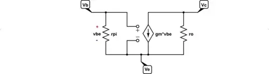
simulate this circuit – Schematic created using CircuitLab
The model only works for a tiny range around a known DC operating point. So the DC operating point's quiescent current \$I_{_{\text{C}_q}}\$ must be found, first.
An operating temperature should be selected so that \$V_T\$ can be determined or else just use a rough value between \$25\:\text{mV}\$ and \$28\:\text{mV}\$. I selected \$V_T=25.9\:\text{mV}\$.
Finally, a guess for \$\beta\$ at the operating temperature and \$I_{_{\text{C}_q}}\$ is needed. Usually a typical value can be found in a chart found on the BJT's datasheet. I chose \$\beta=200\$.
All BJTs have a dynamic slope (tangent to their I-V curve) determined by \$I_{_{\text{C}_q}}\$, called \$r_e^{\:'}=\frac{V_T}{I_{_{\text{C}_q}}}\$. I think it is a bit of a misnomer, defined that way, as \$r_e^{\:'}\$ is treated as though it resides at the emitter tip (hence the e in the name) while being defined mathematically by the collector current.
A better term might be to use is its inverse, \$g_m=\frac1{r_e^{\:'}}=\frac{I_{_{\text{C}_q}}}{V_T}\$. Then \$r_\pi=\frac{\beta}{g_m}=\beta\cdot r_e^{\:'}\$. But \$r_e^{\:'}\$ just crops up as a useful idea (as we'll see, shortly.) It sticks around because it is handy.
Although I won't use it, \$r_o\$ is illustrated on this chart below, taken from Ian Getreu's, Modeling the Bipolar Transistor, 1976 (himself citing W. J. McCalla's earlier paper.) It gives an idea about what it is modeling -- the slope to the right of \$V_{_\text{BC}}=0\:\text{V}\$:
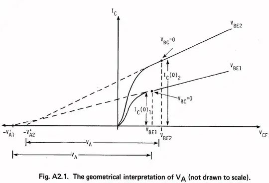
Then \$r_o=\frac{V_A+V_{_\text{CB}}}{I_{_{\text{C}_q}}}\$. (Sometimes this is simplified to \$r_o=\frac{V_A}{I_{_{\text{C}_q}}}\$ or, I believe, also written slightly incorrectly as \$r_o=\frac{V_A+V_{_\text{CE}}}{I_{_{\text{C}_q}}}\$.)
I'm ignoring \$r_o\$ in your case, as \$r_o\$ won't be much of a factor. So, the following analysis doesn't include it.
With that, the small signal BJT model can now be inserted into your circuit:
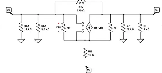
simulate this circuit
Using freely available SymPy and applying KCL to the above I get:
eq1 = Eq( ve/rpi + ve/re, vin/rpi + gm*(vin-ve) )
eq2NoNFB = Eq( vout/rc + vout/rl + gm*(vin-ve), 0 )
simplify(solve( [ eq1, eq2NoNFB ], [ vout, ve ] )[vout]/vin)
-gm*rc*rl*rpi/(gm*rc*re*rpi + gm*re*rl*rpi + rc*re + rc*rpi + re*rl + rl*rpi)
I can define the AC impedance at the emitter, as seen by the collector, as \$r_{ac}=\frac{\beta+1}{\beta}\cdot R_{_\text{E}}+r_e^{\:'}\$. (Just made up the name. But I'm sticking with it here. And here, note, that \$r_e^{\:'}\$ just became useful!)
Then the gain without NFB but including emitter degeneration is \$A_v=-\frac{R_{_\text{C}}\,\mid\mid\, R_{_\text{L}}}{r_{ac}}\$.
The following analysis using SymPy now adds the NFB caused by \$R_{_\text{FB}}\$:
eq2NFB = Eq( vout/rc + vout/rl + gm*(vin-ve) + vout/rfb, vin/rfb )
simplify(solve( [ eq1, eq2NFB ], [ vout, ve ] )[vout]/vin)
rc*rl*(gm*re*rpi - gm*rfb*rpi + re + rpi)/(gm*rc*re*rfb*rpi + gm*rc*re*rl*rpi + gm*re*rfb*rl*rpi + rc*re*rfb + rc*re*rl + rc*rfb*rpi + rc*rl*rpi + re*rfb*rl + rfb*rl*rpi)
Parsing that, in the context of the prior result for \$A_v\$ and the standard NFB equation where \$G=\frac{A_v}{1+\beta_{_\text{NFB}}\,\cdot A_v}\$, I find that the NFB factor can be expressed as \$\beta_{_\text{NFB}}=\frac{\left[\frac{r_{ac}}{R_{_\text{C}}\,\mid\mid\, R_{_\text{L}}}+1\right]}{\left[\frac{R_{_\text{FB}}}{r_{ac}}-1\right]}\$.
In your circuit case, and assuming \$\beta=200\$ and ignoring the Early Effect, I get \$I_{_{\text{C}_q}}\approx 6.2266\:\text{mA}\$ with \$r_e^{\:'}\approx 4.160\:\Omega\$, \$r_\pi\approx 831.9\:\Omega\$ and \$g_m\approx 0.2404\$ for the DC operating point. From these, I estimate \$A_v\approx -4.281\$ (without NFB.) I also estimate that \$\beta_{_\text{NFB}}\approx 0.42664\$. So \$G=\frac{-4.281}{1+0.42664\cdot 4.281}\approx -1.515\$.
The input impedance will be dominated by the feedback resistor. Just divide its value by \$1+\mid\! G\mid\$ and get an estimate of about \$79.5\:\Omega\$. It will be a little lower, of course. Just the \$3.3\:\text{k}\Omega\$ and \$12\:\text{k}\Omega\$ biasing pair alone will drop this to about \$77.1\:\Omega\$. And there will be a little more coming off because of base loading.
I've performed the above calculations without your load resistance included.
To include it, I'll do everything over but this time using the parallel impedance of \$R_{_\text{C}}\$ and \$R_{_\text{L}}\$ (about \$180\:\Omega\$.) Here I get \$A_v\approx -3.50870\$ (without NFB) and \$\beta_{_\text{NFB}}\approx 0.444414\$ and \$G\approx -1.371\$. Input impedance will then be about \$81.692\:\Omega\$. (A little higher than before the circuit was loaded down because now \$G\$ is lower.)
I've not yet run LTspice on these. And I'm frankly a little worried as I'm stretching a simple linearization a bit far. But it's time for verification of the above work product. (I'll set the capacitor values about 100 times higher than you did, just to be sure they don't impact things much.)
First up is the unloaded case:
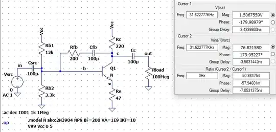
(Note: IKF being set high ensures that I don't get problems with high currents where the \$\beta\$ goes to heck. This will likely mean that the resulting simulation \$\beta\$ will be close to how I set it. And VA being also set very high ensures that we aren't dealing with secondary effects due to the Early Effect.)
Well, here it says \$\mid G\!\mid\approx 1.507\$ vs the above estimate of \$\mid G\!\mid\approx 1.515\$ and that the input impedance is \$\approx 76.82\:\Omega\$ vs the above estimate where I expected it to be slightly less than \$77.1\:\Omega\$.
Next up is the loaded case:
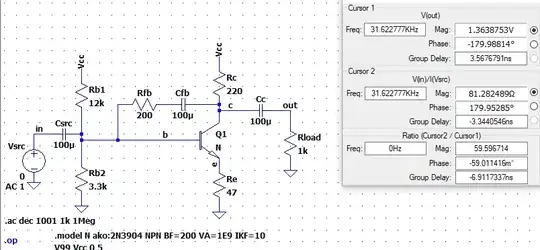
Here it gives \$\mid G\!\mid\approx 1.364\$ vs the above estimate of \$\mid G\!\mid\approx 1.371\$ and that the input impedance is \$\approx 81.3\:\Omega\$ vs the above estimate where I expected it to be slightly less than \$81.7\:\Omega\$.
I'm satisfied.


