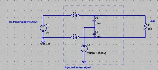
Something like that, yes.
First, you must define what kind, and how much, interference the device should be subject to. This depends on operating environment, product class, and any other considerations, whether at the design level (e.g. commercial FCC/CE ratings would be a prudent starting point) or due to client/customer requirements (automotive, railway, aerospace, etc. projects often stipulate compliance with certain additional regs in the service contract / purchase order).
You would use such a circuit (variously called a bias tee, CDN (coupling-decoupling network), or LISN (line impedance stabilization network) depending on exactly what it's doing) to apply noise to a system, or measure noise emitted from it.
Typical inductor values are 5µH (e.g. automotive), 50µH (per line, mains LISN), 5mH (per pair/cable, using coupled inductors / common mode choke), and so on. Corresponding capacitor values usually around 10nF to 1µF depending on required bandwidth of the network, system impedance (50 or 150Ω most commonly), etc. (Usually when the impedance differs, it's accompanied with a matching transformer, or more often a min-loss attenuator, to couple back to standard 50Ω test equipment.)
Note that impedance of the supply matters; with a circuit as shown, we can add inductance to it, and that's fine if it's already inductive, but we might get unfortunate resonances if the supply has a capacitive output instead, or something more complex (like a long wire pair with multiple resonances besides). It's common to have additional bypass, filtering or damping on the DC/mains port for this reason, hence "line impedance stabilization".
As for signals and amplitudes, and frequency ranges, typical examples are:
- IEC 61000-4-6 conducted immunity: 0.15-80MHz, 3V (RMS unmodulated, 80% AM (1kHz sine modulation))
- IEC 61000-4-5 surge: 0.5-2kV, 8/20 (1.2/50) µs combined-wave generator, 2Ω source impedance (or plus external resistance if higher)
- IEC 61000-4-3 radiated immunity: 80-1000MHz, 3 V/m (RMS unmodulated, 80% AM (1kHz sine modulation))
- IEC 61000-4-4 fast transient burst: 0.5-2 kV 5/50 ns impulse, 5 or 100 kHz repeat rate, 75 pulses per burst, burst period 300 ms
- IEC 61000-4-2 electrostatic discharge, 2-15 kV, 150pF + 330Ω, contact or air discharge, coupling planes, etc.
Note that radiation is applied to the system overall; this results in induced energy on wired connections, on-board traces, etc., and depending on the design, and test levels, can often be modeled as energy conducted through wired ports (connectors, pins, etc.). The same is true of ESD via coupling planes.
Surge is used in specific cases, mainly where long lines can be expected to connect; the effects modeled are inductive kick (particularly from breaking large loads, or faulting circuits), and lightning strike (indirect/induced, or distant). Usually this means mains lines, and telecom pairs.
The effect these various signals have on circuitry, of course varies. Most power circuits won't mind, due to the combination of filtering components (filter modules, iron-core transformers, or rectifier + DC filtering) and scale (a power-switching output isn't usually harmed by ESD). Most ICs are made of microscopic structures that will be harmed by direct ESD or surge (unless so rated; and even then, operationality or reliability may dictate additional protection). Even if not harmed, circuits may malfunction due to invalid signal levels, momentary interruption/interference, etc. The level of severity (A, no change; B, momentary interruption of service; C, persistent interruption of service requiring user action; D, permanent damage) also needs to be specified.
The most important aspect is understanding the differential and common modes, and RF port theory in general. Ground is a global fiction, at best only true locally. Where we have a solid reference plane, at least to the extent we can ignore voltage drop across said plane, anything entering it from the outside can be considered a port, and everything within the plane can be considered safe, immune to outside influence. (Preferably, it's not just a plane, but a closed contiguous surface -- a conductive enclosure, but for finitely many penetrations carrying signals through the shield.)
Circuit ground can be elevated nearly arbitrarily with respect to its surroundings, especially at short (ns, µs) time scales where otherwise intended ground-return paths look like inductors (or other more complex impedance), and wires hovering over the board look like capacitors with suddenly thousands of volts on them, coupling into traces/components on the board indiscriminately.
CM is the reason why a single-side LC filter (just one line to GND, a DM filter) is not a general solution. The circuit board itself becomes embedded in loop(s) closed through external connections, loops which can only be opened by introducing more impedance (CM choke), then the board can be separated from those loops by creating a tighter local loop (in a power supply, 'Y' type capacitors shunt switching noise within the PCB; where isolated comms are used, a 'Y' cap plus CMC might be used for similar reasons; see Ethernet magnetics for example*).
*Not the whole story; actually, the cap is mandatory for ESD immunity, of all things. Which then forces the same ['Y' + CMC] circuit, to meet conducted/radiated.
