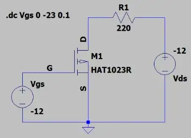
I am trying to understand basics about PMOS transistor such as understand Vth value when the transistor goes to saturation and permits the drain to flow completely. My circuit is this and the voltages are negative but the Voltage Sources (Vgs, and Vds) are placed as a regular circuit with positive voltage values. The ground of the circuit is placed in the same way (similarly when the voltage values are positive).
The PMOS I chose for the analysis is a HAT1023R and according with its datasheet it has a Gate to Source Cutoff Voltage (Vthreshold) of -1.5 V which is consistent with the simulation graphic in LTSPICE:
 At -1.5 V (X-Axis) it reaches saturation zone and flows the maximum Drain Current (Id).
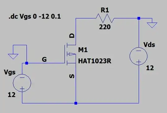
My doubt is about how could I draw the same schematic but with the right Voltage directions something like the following image, but the problem is that both sources are in parallel and produces an overdefined circuit matrix in LTSPICE, I could not understand how could I draw a correct schematic without using negative signs for voltages, somebody could explain me?

