0

The following is differential pair small signal analysis from the book Design of Analog CMOS Integrated Circuits.

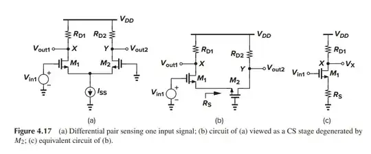
Let us set \$V_{in2}\$ to zero and find the effect of Vin1 at X and Y [Fig. 4.17(a)]. To obtain \$V_X\$ , we note that M1 forms a common-source stage with a degeneration resistance equal to the impedance seen looking into the source of M2 [Fig. 4.17(b)]. Neglecting channel-length modulation and body effect, we have \$R_S = 1/g_{m2}\$ The following is analysis of differential pairs. How can this circuit remove \$R_{D2}\$ in (c)?

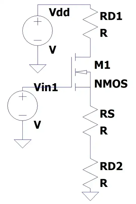
enter image description here

This is what I thought about

enter image description here

kile
  • 798
  • 2
  • 11
  • Can you explain to us why do you think that you should include the Rd2 resistor? Notice that in this case, M2 is working as a common-gate amplifier. What is Rin of a CG stage? – G36 Nov 30 '23 at 13:23
  • @G36 M2 is seen as a resistor $R_S$. Which transistor of $R_{in}$ you are talking about? – kile Nov 30 '23 at 14:30
  • Yes, M2 is seen as a resistor Rs. This Rs resistance is equal to the input resistance of a CG stage. Because in this case M2 is working as a common-gate amplifier. – G36 Nov 30 '23 at 14:54
  • @G36 M2 is in series with $R_{D2}$. Why should we remove $R_{D2}$? – kile Nov 30 '23 at 14:56
  • Find Rin of a CG state (also do not forget to neglect channel-length modulation) and you will see why. Or try to find Rin in a circuit that contains an ideal current source in series with a resistor. And you will see that a series resistor does not influence the current. – G36 Nov 30 '23 at 15:03

1 Answers1

0

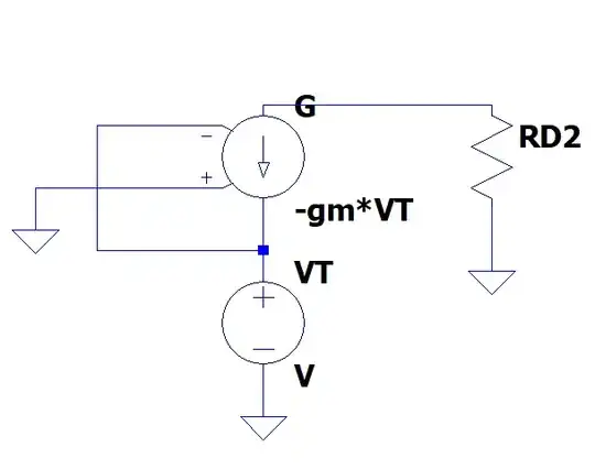
The following is Thevenin analysis.

enter image description here

$$g_m V_T = I_T$$

$$\frac{V_T} {I_T} = 1 / g_m$$

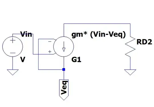
For Thevenin voltage

enter image description here

$$V_{eq} = V_T$$ $$g_m (V_T- V_{eq}) = 0$$ So current source is zero.

kile
  • 798
  • 2
  • 11
  • So, do you see now why we do not include Rd2 in Rin equation? – G36 Nov 30 '23 at 15:33
  • @G36 Thank you. Is Thevenin $V_{eq}$ same as $V_{in}$? – kile Nov 30 '23 at 15:35
  • To be honest I do not understand what you are trying to achieve involving thevenin's voltage here. For what purpose. – G36 Nov 30 '23 at 15:38
  • @G36 In last example we have to calculate Veq https://electronics.stackexchange.com/questions/691011/how-is-cmos-impedance-calculated – kile Nov 30 '23 at 15:40
  • But we do not have to do it here because Vin2 = 0V (M2 gate is at AC GND). – G36 Nov 30 '23 at 15:43
  • @G36 Thank you for you help. I really struggle with analog circuit analysis – kile Nov 30 '23 at 15:53
  • I think that you should focus more on the intuitive understanding of what is going on in the circuit the the math itself. https://electronics.stackexchange.com/questions/355899/how-is-possible-that-with-same-ibase-there-is-more-than-one-vce/355955#355955 ; https://electronics.stackexchange.com/questions/410972/why-is-there-no-phase-shift-in-cc-and-cb-configuration/411171#411171 ; https://electronics.stackexchange.com/questions/301617/bjt-input-ac-signal-amplitude/301642#301642 – G36 Nov 30 '23 at 17:50