Here is a simple step-by-step process:
Step 1. A good starting point is to bias the voltage at Q3 emitter at half the supply voltage, which in this case will be 10V.
So Q3Ve=10V.
Step 2. Next, we select the bias current for Q3 emitter. Let's stick with your existing resistor where R9 = 20Ω. So that gives Q3 emitter bias current of:
Q3Ie = 10V / 20Ω = 500mA.
This means that, with no signal, the power in Q3 and R9 will be 5W for each - I do hope you have a good heatsink for both of these components.. :-)
Step 3. Assuming Q3 Ve is 10V (half of Vcc), we then know that the bias voltage at Q2 base is:
Q2Vb = Q3Ve + 2 x Vbe. Assuming Vbe =0.7V, this gives:
Q2Vb = 10 + 2 x 0.7
= 10 + 1.4
= 11.4V
Step 4. Next, we select the bias current through R7 & R8. Assume that Q2 & Q3 both have DC current gain of 100, then the current gain of the Q2-Q3 Darlington is 10,000. We use this to calculate the base current into Q2:
Q2Ib = Q3Ie / 10,000
= 500mA / 10,000
= 50uA.
Step 5. Next, we choose the current in R7 to be much larger than this base current, anywhere from 10 to 20 times this is usually good. If there are no other considerations to take into account, then I like to use a factor of 20 times, so that means the current in R7 will be:
R7i = 50uA x 20
= 1mA.
However, in this case, R7||R8 will have a loading effect on the previous stage, the Common-Emitter voltage amplifier, which will reduce its gain. The higher this factor, then the lower the values for R7 & R8, which means the more the loading will be, and the lower the voltage gain from Q1. You can reduce the effect of this loading by using a "boot-strap", which I will discuss later. For now, let's assume that the factor of 20 is OK.
Step 6. Next, we calculate the current in R8, which will be 19 times rather than 20 times the base current of Q2 (since the current into the base of Q2 comes from R7 but does not flow into R8):
R8i = 50uA x 19
= 950uA.
Step 7. Now we know both (a) the voltage across each of these resistors, and (b) the currents through them, so we can now calculate resistance values for R7 & R8:-
R7 = (20V - 11.4V) / 1mA
= 9.6V / 1mA
= 9.6kΩ
R8 = 11.4V / 950uA
= 12.0kΩ
Step 8. Now we need to select actual values that you can buy in a shop, so I would suggest using 10kΩ for R7, and 12kΩ for R8. I would not be too concerned at this stage about making R7 to be exactly 9.6kΩ using some combination of series and parallel resistors. You will find that some of the assumptions we have made may have some errors, for example, the gain of Q2 & Q3 may be different to 100, and their Vbe may not be 0.7V (I suspect Q2 may be somewhat less than this, say, about 0.65V, depending on which transistor you use).
Comment
Please check the values you have used for the capacitors and inductor that connect the speakers to the amplifier output. Something does not look quite right there. For example, I would have expected C6 (80uF) to be smaller than COUT (22uF)?
Also, I suspect you will need some capacitors connected from the collectors of Q2 & Q3 to ground. Inductor L1 will filter the current out of the power supply Vcc (which is good), but will cause a voltage "ripple" to the rest of the circuit. To reduce this ripple, place filter capacitors (eg: one or two big electrolytics) from Q3 collector to GND.
Bootstrap:
I mentioned earlier that R7 & R8 present a load on the output of Q1. The R7-R8 bias network will present a load to any signal present at Q1 collector. What happens is that R7-R8 will present as a resistor in parallel with the resistor in the collector of Q1 "RC". The value of this resistance is calculated as R7 in parallel with R8, which we shall call "Rbias". Using the values above, we get:
Rbias = R7 || R8
= 10kΩ || 12kΩ
= 5.45kΩ.
Putting this in parallel with resistor RC, we get:
RC' = Rc || Rbias
= 840Ω || 5.45kΩ
= 728Ω.
Notice that the effective collector resistor of Q1 has reduced from 840Ω to 728Ω (about 14%), which will reduce the voltage gain of the common-emitter amplifier by about the same %.
You can avoid this loss of voltage gain by applying a method called "bootstrapping". We can use the output of the amplifier (at Q3 emitter) to supply most of the current required to drive the voltage at the bias network located at Q2 base. We do this by adding two new components:
- A new capacitor (say, 10uF) connected from Q3 emitter to the join of R7 & R8.
- A new resistor (about 10k) inserted between the base of Q2 and the join of R7 & R8.
Note that the capacitor from Q1 must now connect to the base of Q2. (By the way, you have two capacitors marked "COUT" in the schematic.) The diagram below will give you an idea, this is for a single-transistor CC stage, in your case you have a Darlington so you just connect Cboot to the emitter of the second transistor.
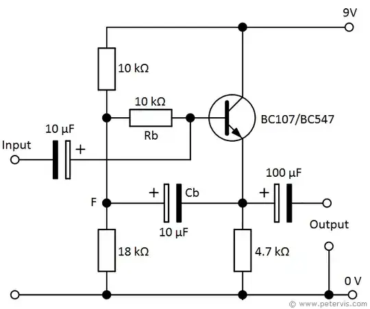
Source of image:
https://www.petervis.com/Radios/bootstrapping/transistor-bootstrapping.html
What this does is allow Q3 to supply most of the current required by R7||R8 to cause the voltage at Q2 base to "swing" with the signal, thus relieving Q1 from this burden. This means that the loading effect of R7||R8 is dramatically reduced, thus reducing the voltage gain loss from 14% to 1% or less.
This new capacitor & resistor, let's call them "Cboot" & "Rboot", "pulls up the voltage at Q2base by its own boot-straps", as the old saying goes, hence the name.
Links to some good information on the "boot-strap" technique:-
https://sound-au.com/articles/bootstrap.htm
Effect of bootstrapping in amplifier circuit

