Is there just a particular type of "flip-flop" circuit that I have overlooked that does this task?
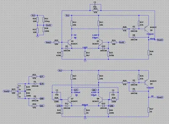
Yes, the flip=flop you want is a toggle flip-flop, aka T-FF. The circuit you found is indeed suitable, but take care when selecting the various components. The image below is a complete circuit using discrete components (no ICs) based on the circuit you found. LTspice simulation shows that it works well, but I have not verified this on a breadboard. It will work OK up to a few kHz - what is the maximum frequency out of your Schmitt trigger?
Description
The circuit is in two parts, the upper part is the Schmitt-trigger buffer (non-inverting), and the lower is the T-FF. The output of the Schmitt feeds the input of the T-FF. Both circuits are based around a common structure: a differential pair followed by a logic inverter, the differences being how the feedback signals are routed.
Schmitt buffer:
A resistor voltage divider provides a reference signal Vref which is applied to the base of Q5; this sets up both the threshold voltage for the Schmitt action, and the bias conditions when there is no signal present (Vsig1 not connected). Feedback is taken from the output of the logic inverter and is applied to the base of Q4. The ratio of R15 (47k) to R19 (22k) sets the hysteresis. C5 speeds up the switching transitions. Diodes D9 and D10 are a precaution: they protect transistor bases from excessive reversed voltage - which is unlikely in a circuit supplied from 5V but may occur as the supply voltage increases. The logic inverter has some diodes that speed-up turn-off, this is commonly known as a "Baker's clamp" (old-school stuff dated from the 1950's).
T-FF:
Hopefully you can recognise within this the circuit you found, with some slight differences. The diff-pair emitter resistor R22 is a lower value (1k vs 4k7), since this circuit will be expecting the input voltage to be logic level about 0 to 5V. Q7 and Q8 collectors are cross-coupled to the base of the opposite transistor via a resistor with a parallel speed-up capacitor. The network shown to the left applies the input signal to the appropriate nodes to obtain the toggle action, as per the original circuit you found. The output of the logic inverter is not coupled to any inputs, so its input can come from either Q7 or Q8. The circuit changes state on the falling edge of the input. Note that the values of C1 & C2 are dependent upon the transition times of the logic edges applied at the input (Vout2); the slower the transition the larger these have to be. When driven by the Schmitt shown here the transition times were about 1us.
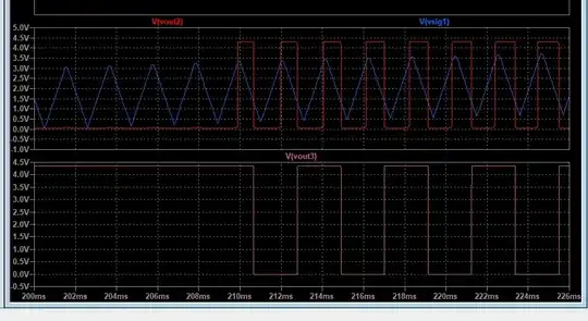
The image below shows the waveforms as the Schmitt output starts to toggle when the input signal comes into range of its thresholds. Vout3 toggles on each falling edge of Vout2.
References:
Adding here some useful resources, starting with oldest first:
Difference between latch and flip-flop?
What values / components do I need in this flip-flop circuit?
How to build a Schmitt trigger using transistors?
Latching Soft ON/OFF Button
How to make this T-flip-flop circuit


