1

I am thinking about how to layout my opto-isolation board. It is used to protect pins on an FPGA, convert signals to RS-422 and then transmit via RJ-45.

I have seen some conflicting information about how to layout optocoupler designs. My understanding is that I should absolutely not connect the two different ground references, but the top related post on this question suggests that I should create a split ground plane that is connected at a small point. I am not happy with this answer because it seems like that violates the isolation by connecting the grounds.

Does anyone have any more insight into this? My initial thoughts were to have a split ground plane layer, where the two sides are not connected at all and are spread apart as far as possible. The connectors relevant to GND_A would be on the left side and those relevant to GND_B would be on the right side, for example.

Does anyone have any insight into the best way to do this?

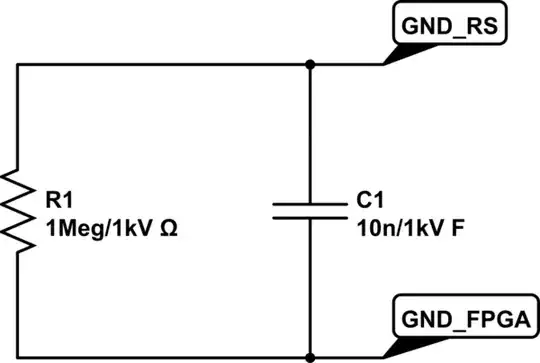
Also if anyone has any feedback on this circuit overall it would be much appreciated:

Edit: I have changed the schematic based on the input in the comments, as I falsely assumed that the VDD1 and VDD2 inputs of the optocoupler were not connected internally enter image description here

Friizzle
  • 25
  • 5
  • 1
    Shouldn't those cathode pins be connected to GND_A? – MiNiMe Oct 29 '23 at 11:11
  • Connected like that, the optocoupler is useless. You have shorted both supplies and both grounds together through the opto. – Justme Oct 29 '23 at 11:15
  • Even worse, both 15 and 16 are GND. – MiNiMe Oct 29 '23 at 11:25
  • @MiNiMe No they aren't. – Justme Oct 29 '23 at 11:35
  • @MiNiMe Ah thank you my bad I didn't spot that! – Friizzle Oct 29 '23 at 11:38
  • @Justme Do you mean the problem with the cathode pins that MiNiMe spotted or something else? – Friizzle Oct 29 '23 at 11:40
  • @FergusRooney If you want to isolate then don't connect supplies and grounds together. If you don't want to isolate then don't put an isolator. – Justme Oct 29 '23 at 11:55
  • 1
    No, @Justme mean that pin 9,10 and 15,16 are not for separate power input. They are internally tied together. – MiNiMe Oct 29 '23 at 11:55
  • @MiNiMe AHH I see thank you! I looked over the datasheet again and you are correct. I had assumed pins 9 and 10 were power for the photodiode and 15 and 16 were for the sensor side, but both sets are for the sensor side. I should connect pins 9 and 16 to GND_B and pins 10 and 15 to VCC_B – Friizzle Oct 29 '23 at 12:16
  • "split ground plane that is connected at a small point" What would that be? – MiNiMe Oct 29 '23 at 12:22
  • @MiNiMe And if it would be connected, what would be the purpose of the isolator any more if it is not used for isolation. – Justme Oct 29 '23 at 12:26
  • @MiNiMe I believe what the poster was referring to is a slit in the ground like this : https://electronics.stackexchange.com/a/306896/353427 , I am asking if it would be acceptable to have a split ground plane that is just not connected at all – Friizzle Oct 29 '23 at 12:28
  • Sure. You got two circuits and signaling between them through an optocoupler. I'm not sure what your reason is, but it'll work. – MiNiMe Oct 29 '23 at 12:34
  • @MiNiMe The purpose is to protect the FPGA pins from overvoltage by ESD events, power supply errors in the receiver circuit or other problems that long cables can produce – Friizzle Oct 29 '23 at 17:31
  • Normally you should connect neither the two grounds, nor the two power sources. Else, why using an optocoupler. The only hypotethical exception when the recieving side has to measure some voltage relative to to the sending side ground. But I can't imagine someone designing such a circuit. – Fredled Oct 29 '23 at 20:03

1 Answers1

3

How the ground's are seperated (if they are) depends on your system design.

Assuming you want full isolation and can supply power to the isolated side via the RJ45 as well, you can do something like this:

schematic

simulate this circuit – Schematic created using CircuitLab

(1) The capacitor C1 helps to "couple" transient events between the grounds. Make sure, that it has a low ESR and a sufficient voltage rating.

(2) The resistor R1 helps to "couple" small dc-currents to avoid huge DC-Voltage offsets. Make sure, that it has a sufficient voltage rating.

(3) Otherwise, do not connect the grounds. But, you should add a additional component to be left unpopulated for measurements or to bridge the grounds during debugging.

ElectronicsStudent
  • 3,489
  • 7
  • 20
  • Ah I see thank you. I was was planning to have the receiver end powered by a separate supply, but I would pass the RS-422 gnd through the twisted pairs and then connect them to the receiver ground – Friizzle Oct 29 '23 at 14:34
  • But why add a coupling cap or leakage resistor? What if there really is constant 500V DC or AC between grounds? The opto can handle transients of 1000V at a rate of 10kV/us. – Justme Oct 29 '23 at 16:32
  • @Justme Well, if both grounds are DC-connected to earth somehow, they will reduce noise afaik. But, i'm no expert. I have seen it in many professional designs over the years (teardowns, replacements, etc...) – ElectronicsStudent Oct 29 '23 at 21:35