I will attempt to answer your questions here. Firstly, some background context collated from the "comments" section (thanks to Sam Gibson, Tim Williams, & Russell McMahon):-
Source of the circuit:
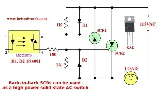
As provided by the OP:
https://www.edaboard.com/threads/back-to-back-scr-driver-circuit.401988/
Original source:
Refer Fig 4 of this link, image copied below:
https://www.bristolwatch.com/ele3/1d.htm
Responding to your questions:
Is this circuit considered to be sufficient for general using in the Market?
No. There are many things missing, just for starters: over-load and short-circuit protection (eg: fuses), over-voltage protection, EMC filters, safety eg: electrical isolation.
what is the use of these two diodes?
Referring to D1 & D2:
(a) They prevent reverse voltage being applied to the G-K terminals of each SCR.
(b) They ensure that the gate trigger current is determined by R2 & the load, and is not affected by R1 & R3.
what is the general snubber circuit is used in Market (for general purpose I need it because I know it should be calculated for specific loads)?
As you indicate, the exact snubber depends on the intended application, the type of load, and the details of the SCRs used. For example, if the mode of operation is to trigger the SCRs only when the applied 220VAC voltage is zero (zero-crossing) then then snubber required will have a lower rating than for random-trigger point-on-wave triggering (where the trigger can occur at any point on the AC cycle). Futhermore, if you intend to use this circuit for dimming lamps (where the trigger may occur at any point on the 50Hz waveform, and is repeated for each AC cycle), then this means the snubber will be working at 100Hz or 120Hz (once in the positive half, and once in the negative half) and this will cause the highest power loss within the snubber (and the SCR). It will also generate the most EMI - which needs to be carefully filtered, the snubber is a part of that EMI filter.
Loads can be resitive, inductive, or capacitive; a purely resistive load will probably have the lowest-rated snubber, whereas a capacitive load will require a different type of snubber compared to an inductive load.
Snubbers are used to:
(a) protect the SCR from over-voltage, & over-current (particularly at turn-on into capacitive loads);
(b) prevent false turn-on (usually caused by high dv/dt across A-K), and
(c) limit power dissipation within the SCR for non-resistive loads.
Please note that different types of SCRs have different values and limits for all these parameters, and these parameters vary with temperature, so the snubber must be designed for the specific SCR being used (and the manufacturing tolerances to be expected), and the operating conditions - ambient temperature, and internal temperature rise.
Is it possible to just use a TVS diode instead of a snubber?
Possibly, but it depends - see the answer above.
Snubber design:
These links may be a good starting point:
Snubber design for switching an inductive mains load with a relay?
How to design an RC snubber for a solenoid relay driving an inductive load??
Designing an RC Snubber for TRIAC motor control?
Update 30-Oct-2023:
Responding to this part of the OP:
Third I will explain the changes that I made:
I changed R1 from 220 Ω to 10 Ω because when I first connect the circuit to live power (without connecting the optotriac to 5 Vdc (Moc 3061 ZVC I am using)) the SCR gets triggered for a fraction of second and gives a pulse of 311 Vac peak (220 Vac RMS) when I changed it to 10 Ω surprisingly it became much more stable and done that for R3 too.
R2 got changed from 500 Ω to 100 Ω because when I changed R1 and R3 to 10 Ω R2 got burned so I lowered it to 100 Ω.
I added a snubber circuit too (R4 and C1)
What you experienced here is known as "the first pulse effect": how the circuit behaves when power is first applied. This behaviour becomes more complex as the number of power sources increases; in this case there are two: (1) the AC supply, and (2) the voltage at the LED side of the opto-coupler. The RC snubber you added has a large effect on this behaviour, and you may find that this snubber has corrected the false triggering that occurred on the first pulse with the resistors R1, R2, & R3 set to their original values.
I would suggest changing resistors to higher values; 10Ω & 100Ω seem too low to me, and may result in excessive gate currents. Check the SCR data sheet. Don't forget also that the optocoupler output stage has to carry this current.
I would also suggest that you take into consideration the "first pulse effect" for the opto-coupler, and consider using resistors to ensure the LED is kept off during the start-up phase; in particular, you must ensure that currents caused by capacitive coupling between nodes with high dv/dt cannot cause unintended turn-on.
Update 02-Nov-2023:
Responding to part of the OP's comments under the OP:
@FabioBarone I have a question mate if you may, now I don't understand why did you suggest that we increase the resistor values of 10 and 100 ohms, I mean are not they safe or would they have low lifespan? and about the Opto-coupler the LED side is already turned off when I connect the circuit to AC power. –
Hazardous Voltage
9 hours ago
My response: Because the current flowing in the opto-TRIAC may be too high.
May I suggest looking at the datasheet and application notes. For example, assuming the opto triac you are using is the MOC3061TVM, and its datasheet is here:
https://www.onsemi.com/pdf/datasheet/moc3163m-d.pdf
Page 6 shows a typical application for firing two back-to-back SCRs (image below):

This suggests making R1=R3 (using the component IDs of your diagram, not those of the diagram above) = 330ohm (or not installed at all, these are "optional"), and R2=360 ohm, and note that this is for a 115V AC supply, a 220VAC supply would need higher values again to keep the current to the same values.
Suggest consider the two cases:
- When the opto LED is OFF (no current). Look at the voltages present on all the components of your circuit.
- When the opto LED is ON (conducting forward current). Look at the currents that are flowing in all the components of your circuit.
The other cases to consider are:
3. The transition between case 1 (OFF state) and case 2 (ON state).
4. The transition between case 2 (ON state, when the main SCRs are conducting load current) and case 1 (OFF state).
For cases 3 & 4 you need to consider in small time steps how the circuit behaves as it makes these transitions. This is when the snubber, and how it interacts with the load, becomes very important. A simulation program, such as LTspice, will be very useful for that.


|| I was just curious as to whether my previous experience with TRIACs & SCRs regarding their differences in dynamic behaviour was still applicable today - these two examples were surprisingly very similar. Cheers. – Fabio Barone Nov 01 '23 at 03:12