Annotated photo:
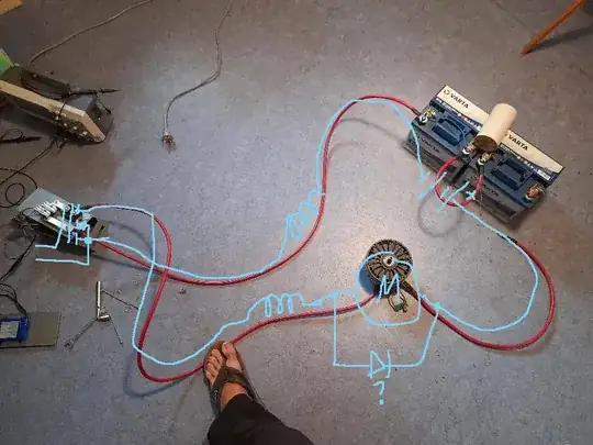
You have a giant inductive loop around the switching circuit.
This is a lesson on seeing wires as what they really are:
All current-carrying paths have inductance proportional to length.
There is also a geometry factor due to how the wires are laid -- they're making a fairly wide loop here; and for the wire diameter relative to the loop width/length. (Capacitance too, but for other reasons, it isn't important here.)
Generally speaking, the inductance is proportional to length times the inductivity of free space, 1.257 µH/m. Typically the geometry factor is 0.2-0.6, so we expect more like 0.5 µH/m for general wiring. I'm guessing the perimeter here is a good 3m or so, totaling 1.5µH, or in that ballpark.
The fundamental equation of inductance is:
$$V = L \frac{dI}{dt}$$
For a transistor capable of switching over a hundred amperes, even if over some microseconds, that's a dI/dt of 20A/µs easily, or a peak voltage of 30V. Maybe not destructive, but dI/dt may peak higher than this as well, and this adds to switching losses. Not to mention, the fraction of this loop inductance near your driver circuit, drops a fraction of its voltage, which likely explains the ringing waveform.
The ringing frequency will be the transistor's Coss with the loop inductance. This is about 2.1nF, giving a resonant frequency of 2.9MHz. Since it looks to be about 1.5MHz instead, either there's more capacitance than that for some reason; or we can assume it instead, go in reverse, and find 5.4µH loop inductance: perhaps the wiring is longer than I think, or the geometry factor is closer to 1 (or even above).
The diode at the motor is doing much less than it could be. It is, at least, clamping the inductance of the motor itself, but it leaves the wiring unclamped, so the transistor has to deal with all of it.
The capacitor at the battery does nothing; in fact the battery itself has quite a lot more capacitance already. Batteries are essentially capacitors with extra stuff (chemical reactions); they're actually pretty good, generally speaking, at short time scales (100s Hz+). The limiting factor (dominant loop impedance) is the wiring inductance.
Remarkably, we can cure all these problems with a simple rearrangement: move the diode and capacitor adjacent to the transistor.
The explanation for this change should be pretty obvious and understandable now: you have an inductive loop in the wiring, and by adding that inductance in series with the motor's winding inductance, you can handle both in one location (at the drive), while keeping switching noise away from the battery leads (not that it matters here, but it would in a professional automotive application, for example).
Wiring inductance should also be kept lower by pairing conductors. You almost always want the positive and negative/return currents paired together, such as by twisting or tying the wires together, or using cable. For three elements spaced apart as shown here (the drive, motor and battery), you should increase the total wiring length just a bit, so that the motor connects only to the drive, and the drive connects only to the battery -- that is, extend the +24V connection from [battery and motor] down to the drive, so the motor inductance can be clamped there, and a capacitor can locally bypass it. This keeps the current loops local and independent, rather than coupling into everything nearby.
You'll probably need a bigger capacitor too (1000s uF), partly to keep ripple voltage down, partly just because ESR has to be small enough as well (~mΩ).
Finally, with a more compact arrangement, you can look into faster gate drive and transistors.
NE555 is only good for ~200mA, and CMOS even less. A separate driver is required.
Discrete circuitry can be used, boosting that to a fraction of an ampere with fairly simple means (e.g. 2N4401/3 emitter follower), or several amperes if you shop around for suitable parts (e.g. PBSS303NX/PX). Among ICs, yeah, a TC4420 would do fine, but take care, specifically because it is so much more powerful, so much faster, than anything you have worked with so far -- instead of meters of wire being a concern, mere centimeters of wire are a problem!
These drivers are fast and powerful devices; not powerful in the sense of making things move like the motor does, no, but powerful on short timescales, timescales that semiconductors are sensitive to. You can easily cause malfunction from stray switching signals, or outright destruction from excess voltage or current peaks.
When you see PCB layout recommendations, heed them well: do not use perfboard or solderless here; use a "deadbug" or "manhattan" style breadboarding technique instead. Use copper-clad PCB as a ground plane, and route connections on top of that. Make nodes by soldering squares of copper clad on top, or cutting out islands in it. The nearby ground plane minimizes loop area, keeping the inductive geometry factor low, and keeping currents in local loops, flowing where you expect them to flow. You also get a nice common ground connection for free, and it's an excellent RF shield and reference plane.
As for faster transistors: first off, there is some folly in choosing extremely low RDS(on) parts. I've seen newbies do this plenty of times, so it bears some discussion.
Now, the reason for that naivete is pretty obvious; newbies likely don't know how to work with the charge and time parameters, so ignore them, and concentrate on what they do know instead (resistors dissipate power, aha!). That's very understandable.
What's interesting is, it's a folly I've seen professionals make from time to time as well; and even myself occasionally!
So let this serve as a reminder: applications are balanced in multiple aspects, rarely if ever just one variable. Here, don't neglect time or charge or speed; model things in SPICE, or measure them on the breadboard, making sure to model strays/parasitics appropriately, like wiring inductance. And to strategize around their effect, like where and how to probe a circuit to get accurate measurements.
As for the underlying cause, then: if you find yourself skipping over datasheet parameters, I mean to be fair -- it might be because you really don't need them (who cares about the body diode here?..). You don't always need every parameter in every application. But also, if you're not understanding some parameters, or not applying/using them correctly, maybe stop for a moment and think about it; look them up, drill down into them a bit more, see how they're measured, how they're used; or ask!
Which, is actually a pretty good exercise by itself: even just finding definitions of datasheet parameters can be surprisingly difficult, let alone how they're measured or used. (The root cause is, more or less, the industry standards they're cribbing from (JEDEC, JESD, etc.), aren't available publicly, so outside of industry, we never really know what they mean, or why they're chosen for a particular part.) Offhand, Toshiba has a good explainer of parameters they use, and older databooks are often a good resource; old Motorola (now Nexperia, NXP and others) datasheets and databooks, and IR (International Rectifier, now Infineon) databooks and appnotes, can be illuminating here. I'll actually intentionally not add citations here, as an exercise to find them. (If such references end up in the comments, or subsequent edits, consider that spoilers, then. ;) )
Anyway, faster transistors -- despite the above discussion, there is still some value in keeping Rds(on) low. Particularly if capacitances are reduced accordingly. Notice Qg(tot) on that IRFP2907 was around 400, 600nC max? Compare to a modern type like CSD19506KCS NexFET | TI with max 156nC. The gate can switch about three times faster for the same drive, but even more than that, the Miller effect has been reduced extremely well in the NexFET family (see how small the notch/step/plateau is in the gate charge plot!), meaning the drain voltage can transition in a fraction of the time the gate does. Which means less gate drive is required; you still get reasonable load-side switching performance with modest drive input. Now, this is still a fairly large transistor (by "large", I mean die area; gate charge is roughly proportional to die area, while RDS(on) is inverse to it -- which is why lower RDS(on) * QG is a figure-of-merit for device performance; power dissipation tracks with die area as well), and I would probably choose a 1-2A gate driver, or a larger one with series gate resistance limiting it to a similar level (i.e. 4.7 to 15Ω). This affords gate transition time in the 200-300ns range, and drain transition time in a modest fraction of that. (Which, again, if we're switching say 50A in 100ns, that's a huge dI/dt that needs very short, and wide, wiring between MOSFET, clamp diode and bypass capacitor!)
Indeed, both conduction and switching losses can be reduced so well with modern devices, they're largely available in SMTs more than THTs. It's hard to sink power out of an SMT assembly; typically these will be good for just a few watts each. But they're indeed capable of tremendous efficiency, so even a 1kW motor drive can dissipate just a handful of watts, with thermal pads coupling PCBs to heatsinks or the enclosure, and that'll do.
But, as I'm sure you can guess -- it takes quite some engineering to pull off something so precise, to be handling thousands of watts while dissipating dozens. One slight misstep and the whole thing explodes (hundreds of amperes of fault current are available from the battery, nothing a tiny silicon chip can survive for more than hundreds of microseconds!). You will be more comfortable with larger devices, capable of dissipating some power, and switching them a bit more slowly (fractional µs should be okay with modest layout). And it's not like you need to switch the motor at 100s of kHz,a few will do, so the switching speed doesn't need to be anything crazy. Just make sure the switching happens all in one place, keep the MOSFET-diode-bypass loop short, and you'll be sitting well.
Once you have the basic PWM drive down, perhaps study current mode control next? :) Complexity: modest, some comparators and op-amps; advantage: continuous torque control/limiting, complete prevention of locked rotor or inrush surge currents; greatly reduces risk of catastrophic transistor failure!
Cheers and good luck.
Here is an example layout, on PCB, top-down view:

Notice the components are about as close together as possible. A few mm here and there won't be a problem, but the important part is a distance of ~cm between them rather than ~m.
The +V and GND connections are a sandwiched pair over almost the entire board area: the conductors are very wide, and narrowly separated (i.e. by board thickness, ~1.5mm). A small exception to the +V area is the switching/output connection, which is similarly wide. Note that the gate drive connections should be the only ground connection between the control and power circuits; avoid making other ground connections between them, which would create loops.


