13

Well, this is a toughie -- though fairly simple. Does anyone have experience with board twist affecting your circuit?

We have a board design that is supposed to measure a loadcell. We have finally tracked a system accuracy fault down to the amp IC. When we twist the board, the amp IC changes its output.

_

Added RM:

Circuit:

enter image description here

Datasheet here

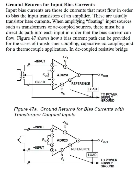
Gain is 100,000 / R7 =~ 454.5 according to datasheet p15.


I get +80mV when I twist the board from its 4 corners. I'm using the amount of twist that I use to unlock my car with my car key. I get -80mV when I twist the other way. The amount of twist is proportional to the variance in output voltage.

Alternatively, if I put, say, typical pencil pressure on the top of the IC, I get +20mV. This is the most sensitive corner of the IC near pin 1.

To isolate the amp circuit, I have shorted its input and disconnected other circuits from it so that what you see in the diagram is what we're testing with.

I'm stuck. What physics principle would cause this? How can I prevent it?

Notes:

  1. This is a system fault, not a single-board fault. It happens on all our boards.
  2. I have tried re-soldering the pins. That's not the problem.
  3. It isn't the gain resistor R7. I've put that on long leads to test its twist separately. Twisting it doesn't make any difference.
  4. The resistor R7 is 220 ohms which equals an amp gain of 456
  5. The power supply rail, AVdd, measures steady at 3.29V
  6. The IC is the industry-standard AD623ARM (uSOIC package)
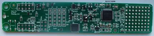
  7. For those who really must see it, here is the board -- though I'm afraid that it will raise more red herrings than answers: enter image description here
Berwyn
  • 363
  • 2
  • 8
  • 3
    If you can, a photo of the board would help us see physical factors that could contribute to the issue. Are the passives leaded or smt, and what size? Where is the circuit located on the board, in the center or near an edge? – The Photon Apr 23 '13 at 05:20
  • 1
    I'd guess you ARE measuring a load cell - made with copper tracks, although the voltages seem far larger than reasonable. As shown your IC has no common mode restraint on the input circuit (pins 2 & 3, shorted). Look at the datasheet table 8 page 21 and the several pages of related comment preceding it and ensure you are not violating any limits there.(THey MAY just be putting common sense in a complicated way - hard to be sure without wading through it. My wife says its time to go and buy the Subway 12" special offer, so ...) – Russell McMahon Apr 23 '13 at 05:58
  • Re: " ... Good point. I should have shown on the schematic that my shorted inputs are still connected into the 350 ohm loadcell bridge. So that should take care of this problem. ..." Good. Another step forward. In a few more days we may have half the circuit diagram :-). It would be 'really wise' to show us the circuit in entirety at least as far as all voltages and currents are concerned. What is the value of AVdd. What is the load cell voltage (AVdd?) and what is the mean DC input voltage (AVdd/2, AVloadcall/2, AV...?) None of this may be of any relevance. All of it might be. – Russell McMahon Apr 23 '13 at 07:58
  • Goodie? You don't need a load cell; just convert the input force to a board twist. :) – Kaz Apr 23 '13 at 21:13
  • Rebuke accepted, RM. I tried to present the real minimal test circuit but I missed some. I have updated the schematic to include the loadcell even though it is shorted. – Berwyn Apr 23 '13 at 22:29
  • Again, can you describe the problem? I know the output changes when you twist the board, but that hardly constitutes normal use. In real use, the board is mounted, and the forces on it are constant. What problem did you see that made you look for causes in the first place? Unknown and unaccounted for static offsets? Dynamically changing offsets? – Scott Seidman Apr 23 '13 at 23:30
  • The overarching problem is that we're trying to eliminate error factors as we have noticed they effect our calibration. The board is not securely mounted while being calibrated, and we didn't realize that would cause an issue. But while doing our calibrations, we noticed that merely turning the board up-side-down affected the reading ... leading to our discovery that board twist affects the reading. We can work around this with secure mounting now that we know about it, but we wanted to understand the cause better first. – Berwyn Apr 24 '13 at 02:18

6 Answers6

14

There are known effects like this that need to be taken into account for high precision circuits. Thermal gradients can also have adverse effects, component orientation across or along stress and thermal gradients etc.

Of course we have to do some guessing because we can't magically know what is in the package. But an educated guess is that the die is either eutectic bonded or glued very rigidly to the bottom of the package cavity. A small SOIC package is very non compliant (i.e. rigid) so the stresses translate directly into the package die cavity floor and then through the die attach into the Si substrate. Stress can adversely affect Si performance by affecting the electron/hole mobility and Si has known piezo resistance (through similar effects of lattice changes).

In fact Intel uses localized stress to increase the performance of PMOS transistors at some process nodes. In laying out precision circuits in silico it is recommended that sensitive amplifiers in Si not have metal layers over them so that the transistors are not adversely affected. (but here it is a matching issue).

to test the hypothesis: I recommend desoldering the amplifier, and then attaching short stubs of PTH (resistor would work) leads to lift the package up off the PCB so the stress doesn't translate into the package. Once you've fiddled with this and re-fired it up. You should see a change and therefore a verification. USe the new "legs" as compliant members. Or use solder braid if you want to get really carried away.

Solutions? a DIP version of the same part will have less of an issue because the leads are compliant. In that case using a compliant thermal compound under the package to get heat out might be used.

You should also consider your board design as a contributing factor. Perhaps running stiffeners (in the existing design) as a test will help eliminate/study the issue. I'd epoxy stiffer pieces of FR4 (on edge) just to see.

placeholder
  • 30,170
  • 10
  • 63
  • 110
  • 1
    The micro package of this chip has particularly bad offset specs, in fact. If I needed to remake the board to accommodate a DIP, anyway, I'd consider moving to the AD8230 auto zeroing inamp if offset is key to this design. – Scott Seidman Apr 23 '13 at 15:19
6

You have a fairly large gain on the op-amp. The 80mV you see corresponds to about 100uV on the input! Anything you do that puts an extra 0.1mV on an input will explain your observation. Even just touching the board in the wrong place might do this.

The simple answer is "don't twist the board". Mount it in a way that this isn't the issue, maybe by one corner.

I'm curious. Are you seeing a static problem, or a dynamic problem? Mounting a board is a static thing, that shouldn't change over time. The Input offset (if that's what it is) that you're seeing when you twist the board is well within spec for the AD623 at this gain. If a STATIC 80mV on the output is a problem here, you've specced the wrong chip. That's not to say that you expect a mechanical intervention to change the input offset, of course, merely that a static offset of this size is expected with this IC.

Scott Seidman
  • 29,939
  • 4
  • 44
  • 110
  • +1 for pointing out the chip is still operating within spec. – The Photon Apr 23 '13 at 14:56
  • It's a static problem. And yes, we can solve it by holding the board still. But we noticed this issue in calibration when we weren't yet holding the board very still, and I wanted to know what caused it. – Berwyn Apr 25 '13 at 01:34
6

Some of the other answers have some good suggestions, but here's one more. When I hear that physical stress is changing the performance of a circuit, I immediately suspect capacitors on the board. Capacitors are notoriously sensitive to stress, and can easily induce signals into precision circuits like this due to stress or vibration.

However your circuit as drawn doesn't contain any capacitors in locations where they should be able to do this.

That makes me think there's some capacitors in your circuit that you haven't drawn.

The one that comes to mind is the parasitic between the inputs of the amplifier (pins 2 and 3) and any nearby power or ground planes. It's common practice to put openings in the power and ground planes below any high impedance nodes in a precision circuit like this. In the case of the AD623, the inputs have about 2 Gigohm equivalent input resistance, and you're also applying a high gain to any signal induced (differentially) on those pins.

If you didn't cut power/ground away from below your AD623 input pins (and any copper connected to them), then board stress will change the value of the parasitic capacitance, causing charge to move around, and I could imagine this creating the kind of offset signals you are seeing.

This hypothesis is somewhat less likely to be right given that you're testing with the input pins shorted together, but I would check it if the other issues don't prove out.

The Photon
  • 129,671
  • 3
  • 164
  • 309
  • I don't think this is the problem. There were capacitors in the original circuit, but I have removed them for this test -- and that made no difference. There is no power or ground plane. – Berwyn Apr 23 '13 at 22:46
5

Ok, let me summarize. The answers re 'strain gauge effect' or the effect of silicon stress on mobility seem to be correct. The effect of the stress on the inputs is multiplied by the gain of the amp.

I have completely removed the package from the board and tested it without a board by wiring leads from it to a bread-bard. Stress on the chip alone still has the same effect.

My further tests show that the uSOIC package that I'm using is about 10 times worse (more sensitive to stress) than the DIP package. This is consistent with the datasheet's specified variance for the uSOIC part. I think I can use a standard SOIC next board spin.

Berwyn
  • 363
  • 2
  • 8
2

Some of my friends provided the following two answers that I will include for reference:


[Greg Bauer]: I wonder whether this is due to a deformation of the IC (as you are no doubt thinking) which is resulting in an equivalent pressure gauge or strain gauge reaction in the silicon of the front end of the amplifier. As the amplifier will have its own differential inputs any affects that unbalance that input will cause a variance in the input offset voltages which are then amplified (by open loop gain?) then on to the output.

I might have to think about this a bit more.

I know that in the olden days when semiconductors were rocks and dinosaurs reigned that if you put pressure on either the silicon piece in a 2N3055 or an LM301 op amp you got some interesting effects – in fact sound wave pointed at an old school metal can LM301 with lid removed would pick up like very very incredibly very poor microphone (was playing with these op amps back in ~1976).


[Gary Anderson]: It sounds like you're operating your amplifier as a strain gauge. When you twist the board you will also be twisting the amplifier die which will cause slight changes in the resistors within the amplifier. The 80mV swings are within the spec for this part. (200µV input offset voltage times 454 = 90mV.)

Do you have a problem with bending of the board in its application? If so you may need to route slots in your board to destress the sensitive parts. Best not to bend the board.

Berwyn
  • 363
  • 2
  • 8
0

You can't expect to do a sensible test with the AD623 configured in your circuit diagram. Although you have inputs shorted together they need to have the ability to "release" their respective input bias currents to ground: - enter image description here

I'm not saying that your real working circuit is problematic in this area - just your test setup. However, if your "proper" circuit does not have components that can remove these bias currents you will have these sort of problems.

Andy aka
  • 456,226
  • 28
  • 367
  • 807
  • Good point. I should have shown on the schematic that my shorted inputs are still connected into the 350 ohm loadcell bridge. So that should take care of this problem. – Berwyn Apr 23 '13 at 07:40