Why is everybody discourage from this paired NAND BJT Transistor "design"? I already saw a few posts where somebody asked something about the paired BJT NAND "design" and the answers only say: don't do it like this, use only one transistor and as many resistors as you want on the base for the inputs?
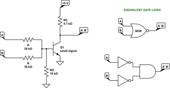
When I refer to the one/two BJT circuits, I mean these:
One BJT NOR:
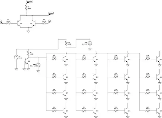
Two BJT NAND:

To list a few:
- https://electronics.stackexchange.com/a/72416/334371
- https://electronics.stackexchange.com/a/281320/334371
- https://electronics.stackexchange.com/a/300116/334371
And a further question, isn't the one BJT Transistor "design" bad, because current can also flow out of the gate input and interfere with other gates?