3

When should I connect the shield of my cable to the PCB ground plane and what effect will it have?

In addition, what effect do those shieldings have on EMI, does the shielding block out HF or LF noise?

enter image description here

This device connects to my PC. It has a plastic enclosure.

winny
  • 14,707
  • 6
  • 46
  • 66
JoeyB
  • 2,177
  • 17
  • 47
  • 4
    There is no one true answer to that, because it depends on so many things. It depends on if your product is the host or device, does it have metal case or plastic, does it have other connections to outside world or not, and whether you have EMI problems and need to pass EMI tests before selling the product. – Justme Jan 14 '23 at 22:28
  • @Justme this device connects to my PC. it has a plastic enclosure. It does not have any other connections. Is there a book or video that will answer this question or does it just come with experience? – JoeyB Jan 14 '23 at 22:42
  • In that case, it may be a poor idea to connect ground to shield. Yes, books, videos, application notes and reference designs exist on both EMC compatibility and USB interface design. – Justme Jan 14 '23 at 23:14
  • @Justme Can you provide a reason why it is considered a poor idea. – JoeyB Jan 14 '23 at 23:23
  • Please add the additional info to your question by editing it. Is it more like a computer mouse (long chord) or like a memory stick (no chord at all) ? – tobalt Jan 15 '23 at 08:01
  • @tobalt long cord – JoeyB Jan 15 '23 at 21:30
  • This may be of interest: https://electronics.stackexchange.com/a/649065/311631 while the question concerns application of CMCs, the electrical situation is identical to the question of shield grounding. – Tim Williams Jan 15 '23 at 21:41
  • 1
    The cable shield is supposed to extend the faraday cage of the device. But it’s plastic… Beware the shield can act as a receiving and sending antenna, connecting to the return plane can do more harm than good. Read tip: shielding grounding of Ralph Morrison. – RemyHx Jan 15 '23 at 21:58
  • @RemyHx the outer part is plastic but the inner part is metal shielding of the cable. I am assuming by connecting the shield to the ground plan, would introduce noise in the "ground plan" which will couple to my RX, and TX of the chip. Is this explanation correct? – JoeyB Jan 15 '23 at 22:08
  • 1
    The ground plane of the PCB is topologically equivalent to a shield -- albeit a poor one with large holes in it and a low profile. As such, there's not great attenuation between radiated fields and components/traces on board. But it's much better than nothing; and as it happens, it's more than adequate for commercial purposes with average circuitry. You absolutely do want to tie shield to plane, at RF frequencies. Failure to do so invites 100% of radiation in/out of the cable; you literally defeat almost the entire purpose of the cable's shield. – Tim Williams Jan 15 '23 at 23:27

3 Answers3

1

I am a proponent of not mixing Shield and Ground functions. By "ground", I mean here the return conductor for the USB-VBUS power rail, most of all, but also the return conductor for the common-HI/LO USB data symbols.

That implies that there is no node on your device that could take over the Shield function. Such a node, would be a metallic enclosure, for example.

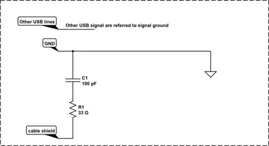
So my suggestion is: Don't connect the cable shield to the ground. However, leaving it open is also not a good practise in a long chord, because its open end can resonate with random noise on the cable.

You want the cable shield joined with your device ground at RF, but separated at low frequencies, so you place a capacitor there. The series resistance is there to damp resonances.

schematic

simulate this circuit – Schematic created using CircuitLab

tobalt
  • 21,701
  • 22
  • 90
0

When should I connect the shield of my cable to the PCB ground plane and what effect will it have?

When you don't have a chassis ground available (such as a USB device in plastic enclosure, you may want to connect them together. It's rarely advisable because ESD will affect the PCB ground plane and could cause resets/issues with digital electronics.

In addition, what effect do those shieldings have on EMI, does the shielding block out HF or LF noise?

EMI can travel up the cable so if you connect shield to PCB ground you can turn the cable into a radiator.

Voltage Spike
  • 82,181
  • 41
  • 84
  • 220
  • "It's rarely advisable because ESD will affect the PCB ground plane" -- I'm not sure what else you would suggest; ESD can't exactly be insulated away! (That is to say: if it would affect other electronics onboard, it will regardless whether you connected a tiny bit of metal to the board or not; the solution is to treat victim circuits individually and as needed.) Likewise, any connection that delivers normal or common mode signals, will become an intentional radiator if no reference plane (shield/ground) is provided for it. – Tim Williams Aug 04 '23 at 18:48
  • Chassis ground, route it around the PCB, if its available. I never suggested to disconnect the shield – Voltage Spike Aug 04 '23 at 20:06
  • @TimWilliams in a chassis-less scenario, I wonder whether introducing an extra PCB ground layer and applying the conventional chassis ground design rule to that layer (e.g. both layers tied at the I/O area) can simulate the beneficial effect a chassis ground using the PCB itself, namely to encourage the ESD/EMI current to flow on the chassis, reducing the injected current into the circuit ground. You can even make a 360-degree shield by adding a cage at the top. But this approach is obviously too wasteful to see any practical use so it's by for not investigated by anyone. – 比尔盖子 Sep 04 '23 at 13:46
  • @比尔盖子 Like an extra layer on top and bottom? (Would that also use buried vias or HDI?) Or a perimeter? A perimeter used to mount a shield would be usable, yeah. Though I don't see a lot of merit in separating the circuit within (leaving a slot between circuit GND plane proper, and the shield boundary). Maybe if you have to manage DC/LF ground loops, and don't mind the cavity/stub resonances thus created? – Tim Williams Sep 04 '23 at 13:52
-1

Let's take this PCB design as an example.

enter image description here

The copper plane under the connector (bottom of picture) and the connector shell have created a Faraday cage effect with the USB cable shield. The signals inside the USB cable are protected from external interference. You will notice that there is no connection between the USB shield and GND.

But remember at high frequency, even if you don't connect the USB cable shield to the GND (0V plane) of your PCB, stray capacitances will. If a disturbance occurs on the cable shield (ESD discharge, common-mode current) it will pass from the shield to the GND (0V plane) via the stray capacitances.

enter image description here

A connection via stray capacitors is by nature uncontrollable, so it is often preferable to offer a controlled path as the @tobalt's circuit or a direct connection between shield and GND

To eliminate the need for a connection between the shield and GND, the Faraday cage should surround the entire device.

Source of image: https://mm.digikey.com/Volume0/opasdata/d220001/medias/docus/742/BOB-15100_Web.pdf

winny
  • 14,707
  • 6
  • 46
  • 66
Vincent
  • 1,122
  • 1
  • 5
  • 13