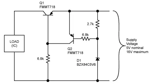
Figure 1. The circuit from the application note.
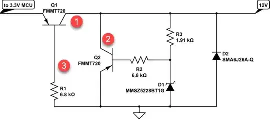
Figure 2. The OP's circuit.
Here are the most obvious errors in your circuit.
- Q1 is back-to-front. Supply should be connected to the emitter.
- Q2 is upside-down. The emitter should be connected to the incoming supply.
- You've missed this connection so D1, D2, Q2, R2 and R3 are doing nothing for Q1.
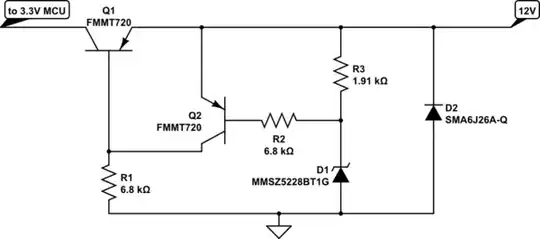
Update since the schematic has been fixed:
From the How it works section,
The transistor Q2 acts as the control element for Q1 and will turn on (turning Q1 off) when the voltage at the power-supply input is equal to the sum of the zener voltage, due to diode D1 and Q2's own VBE voltage at a collector current of about 650uA. Q2 and D1 together produce a typical trip voltage of 5.85V at 25°C. Approximately 0.53V of this is due to the VBE voltage of Q2. The remaining 5.32V is produced across D1. Note that the zener diode D1, although a nominal 5.6V device, is being operated at a very low reverse current, about 200uA as defined by the VBE of Q2 together with the 2.7k resistor.
This is telling you that the circuit is designed to switch off the output if the input rises above 5.85 V to protect a circuit with a nominal 5 V power requirement. You have modified the circuit so that it will switch off when the input voltage rises above 3.9 V + 0.53 V.
As has been pointed out more than once in the comments, This circuit is not a voltage regulator. It is an over-voltage protection circuit.
But when 12 V input is used, MCU Vdd pin only receives around 1 V.
Since 12 V > 3.9 V + 0.53 V the protection turns off the output. The circuit is working as intended by the original designer.

