2

I used the below schematic to output a constant current (~0.92 A) on the RLoad. I turn on/off the N-channel mosfet:

schematic

simulate this circuit – Schematic created using CircuitLab

While current flows through the RLoad, if I tweak the power supply voltage (from 8.53 to 6.8), I notice that the reference voltage (1.25 V at ADJ pin), changes like so:

excel voltage deviation

voltage deviation graph

It might be a deviation of 4 mV or less on the ADJ pin, but I wanted to know why this peak on Adj voltage is happening at ~7.19 V.

I started looking at LM1085's datasheet and the only thing I suspect is the ripple rejection vs frequency. My power supply might be changing frequency on different output voltages.

ripple rejection vs frequency LM1085

My question is: Is there any data/graph on the LM1085's datasheet that describes this behavior? I do not see any input voltage vs ADJ pin graph for example.

Note: I do not think that using the N-ch mosfet creates the above voltage swing on the ADJ pin, since the ADJ is referenced to the LM1085's output pin, and not to GND.

Transistor
  • 175,532
  • 13
  • 190
  • 404
Christianidis Vasilis
  • 3,270
  • 2
  • 9
  • 39

3 Answers3

3

The difference between 1.245 V and 1.249 V is 0.3%. This is pretty good stability for a system whose temperature could vary significantly as the input voltage changes.

Assuming the MOSFET had negligible 'on' resistance, and RRef and RLoad maintained the values shown, the voltage across the regulator varied from ~ 2.17 to 3.91 V, corresponding to a power dissipation of ~ 2.0 to 3.6 W. Assuming a bare TO220 package with thermal resistance from junction to ambient of 22.8 °C/W, and air temperature of 20 °C, the junction temperature varied from ~ 65 to 102 °C, a difference of 37 °C.

The datasheet shows a 'typical' voltage change of about 0.2% between 50 °C and 100 °C, but transient effects could be higher. If you did not allow enough time for the temperature to stabilize then the voltage could have varied as the regulator warmed up and/or cooled down between tests.

Note: I do not think that using the N-ch mosfet creates the above voltage swing on the ADJ pin, since the ADJ is referenced to the LM1085's output pin, and not to GND.

If the FET has negligible voltage drop when on then this should be true. If it didn't then the regulator could have been running close to dropout, causing poor regulation. A similar effect might occur if the power supply had high ripple. I recommend using an oscilloscope to check for ripple and other effects (oscillations, noise etc.).

Bruce Abbott
  • 56,322
  • 1
  • 48
  • 93
2

There is a minimum I(out) requirements you are not meeting in your circuit ...you need a typical minimum of 5mA (max 10mA) flowing from the output pin at all times. Using this type or regulator as a constant current source requires it to be ON at all times. If you switch it off then the internal linearity is not guaranteed and you will get overshoot current at switch on.

You need to add a resistor (R1) as shown below to ensure you meet the required I(out) minimum on a continuous basis.

schematic

simulate this circuit – Schematic created using CircuitLab

Jack Creasey
  • 21,729
  • 2
  • 15
  • 29
  • 1
    Useful thanks!. But I think its not "breaching", right? In a sense that, the datasheet says that this is the minimum output current where it can regulate the output properly. It wont heat or hurt the IC if I dont meet the lower output current while its switched off. It will just create a overshoot when it opens. – Christianidis Vasilis Jun 07 '22 at 06:56
  • If you simply don't like 'breaching' then I can change to another word. I am surprised you'd accept the overshoot on turnon. – Jack Creasey Jun 07 '22 at 20:24
  • Well I wouldn't accept the overshoot, I will for sure add that resistor. – Christianidis Vasilis Jun 08 '22 at 06:57
1

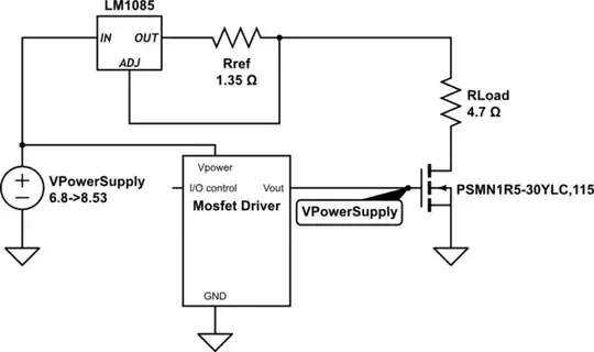
To find the source of this fluctuation in \$V_{REF}\$, we first need to understand what currents are at work here.

On page 6 of that datasheet you'll find \$I_{ADJ}\$ and \$\Delta I_{ADJ}\$. These refer to the current being sourced by the ADJ pin of the regulator, and the low value of \$\Delta I_{ADJ}=0.2\mu A\$ suggests that \$I_{ADJ}\$ is fairly constant at 55μA, but may vary somewhat around this value.

Kirchhoff's Current Law (KCL) requires that this current combine with the current \$I_{OUT}\$ at the junction between \$R_{REF}\$ and \$R_{LOAD}\$, like this:

$$I_{LOAD} = I_{OUT} + I_{ADJ}$$

Rearranging that to find the current \$I_{OUT}\$ through \$R_{REF}\$:

$$I_{OUT} = I_{LOAD} - I_{ADJ}$$

Let's assume (incorrectly) that the regulator manages to keep \$I_{LOAD}\$ constant at the target value of 0.92A, and that consequently the voltage fluctuation you see across \$R_{REF}\$ (which is proportional to the fluctuation of current \$I_{OUT}\$) is due entirely to a variation in current \$I_{ADJ}\$.

The fluctuation in \$I_{OUT}\$ is:

$$ \Delta I_{OUT} = \frac{V_{REF\_MAX}}{R_{REF}} - \frac{V_{REF\_MIN}}{R_{REF}} = \frac{0.004V}{1.35\Omega} = 3mA $$

This is clearly far greater than \$\Delta I_{ADJ}=0.2\mu A\$, and the conclusion can only be that the majority of the variation you see in \$V_{REF}\$ has nothing to do with \$I_{ADJ}\$. In other words, this regulator is not regulating perfectly, and our earlier assumption that \$I_{LOAD}\$ is being pefectly maintained at 0.92A is wrong.

If \$I_{ADJ}\$ is truly constant at 55µA, changes in \$V_{REF}\$ must actually be due to imperfect regulation, and you would see a similar percentage error in \$I_{LOAD}\$. That error is about:

$$ \sigma = \frac{3mA}{0.92A} \approx 0.3\%$$

That's better than the datasheet's quoted load regulation of 1%, but is far from perfect, and illustrates why this particular characteristic of regulators is always included in the datasheets.

As to why this happens, there are many causes, but the big ones might be:

  1. Finite output impedance, which is not constant, and is related to (but not necessarily proportional to) load current. This effectively appears in series with \$R_{REF}\$.

  2. Imperfect internal voltage reference. The designer intended to mitigate this source of error by using a constant current source to drive his reference zener diode (hence the constant value of \$I_{ADJ} = 55\mu A\$) but that can't completely eliminate reference errors.

  3. Non linearity in the reulator's error amplifier, which arises from things like input bias currents and offsets and finite gain, all typical problems you encounter in control systems using op-amps.

While I think your experiment is great, and everybody should be doing things like this, I don't really trust your graph, because there aren't enough data points. It looks quite chaotic, and the lack of a smooth curve here really puts into question your claim that there's a peak at \$V_{IN} = 7.19V\$.

If you made more measurements around that value, which resulted in a smooth(ish) curve around that point in the graph, I would have more confidence in the claim.

Also, I don't know the quality of your test equipment. If for example you are using a multimeter with 1% accuracy, you can't really trust the third digit. This is particularly important here, where changes in \$V_{REF}\$ are of the order of millivolts. When measuring a signal on the 2V range of your DVM, you would need accuracy of 0.05% or better to have any confidence in the 4th digit, which would represent millvolts.

Simon Fitch
  • 34,939
  • 2
  • 17
  • 105