3

The idea is to (almost) replicate the soft power button on a modern PC, using an ATX power supply and some GPIO's from a microcontroller that's going to be there anyway:

schematic

simulate this circuit – Schematic created using CircuitLab

  • With power off, the gates of both transistors are pulled to 0V, which has Q1 off and Q2 on.
  • When the power button is pressed:
    • It grounds the ATX enable pin via Q2, which turns the supply on.
    • Early in the init code, the MCU pulls GPIO_0 high, which turns on Q1. This allows the button to be released without dropping the supply.
    • Later in the init code, the MCU pulls GPIO_2 high, which turns off Q2. This converts the power button into an ordinary user button that is attached to GPIO_1 (internal pull-up), with its ground path via Q1.
  • To power off, either:
    • De-power the MCU, which makes all GPIO's Hi-Z. The circuit then returns to the normal powered-off state.
    • Hold the power button long enough to trigger a software timeout. The MCU then pulls GPIO_2 low, followed by GPIO_0 low, and waits to lose power. Actual power loss happens when the button is released.

Is there anything I should be aware of, that would make it not behave like that, or damage something?

AaronD
  • 5,666
  • 11
  • 37

4 Answers4

3

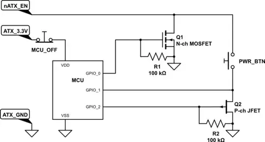
When the thing's powered up and and the PWR_BTN is being used as a user button, you take GPIO_2 high which you say "turns off Q2". I would expect, when you take GPIO_2 high, Q2 will not turn off until it has pulled GPIO_1 way down towards 0V. I would expect GPIO_1 to sit close to ground when GPIO_2 is taken high even without the PWR_BTN being pressed.

EDIT

For a p channel jfet the source is always the terminal which is at the more positive voltage of the two non-gate terminals.

The jfet is a depletion device which means that it is passing maximum current when the gate voltage is equal to the source voltage and, for a p-fet, the current conduction reduces more the further the gate is taken positive relative to the source. If the gate is taken far enough positive relative to the source then pinch-off is achieved where source to drain conduction ceases.

Usually care must be taken with jfets not to forward bias the gate diode. For a p-jfet care must be taken not to take the gate more than about 0.7 V negative relative to the source or the gate diode will be over driven and the jfet may be damaged.

The above describes the operation of a p-jfet. For a n channel jfet just reverse everything.

For an n-fet, the source is always the terminal which is at the more negative voltage of the two non-gate terminals. Again, being a depletion device the jfet achieves maximum drain to source conduction when the gate voltage is equal to the source terminal voltage. Conduction reduces more as the gate is taken negative relative to the source until the gate is taken sufficiently negative to achieve pinch-off at which point drain to source conduction ceases.

As with the p-fet, care must be taken to avoid damaging the fet which, for an n-fet, is likely to occur if the gate diode is forward biased which will happen if the gate is taken more than about 0.7 V positive relative to the source.

My interpretation of your circuit is that when you take GPIO_2 low you are forward biasing the gate diode but this shouldn't be a problem because the source terminal can follow the gate terminal but a small voltage above it, with a voltage drop across the microcontrollers internal pull-up resistor. If instead the p-fet's source had been hard wired to +3.3 V then I would have thought that taking the gate to 0V would have been a problem as too large a voltage would have been applied across the forward biased gate diode. With a typical microcontroller pull-up resistor value of say 20k ohms I would expect the current to be so low as to cause a quite a low voltage drop across the forward biased gate. If a much lower value of pull-up resistor was used then I would expect a larger voltage drop of say 0,7 V across the forward biased gate.

The problem I think I can see is that when GPIO_2 is taken high, if the source were to be pulled-up high by the internal pull-up resistor then the gate would be at the same voltage as the source, the p-fet would be fully turned on, current flows through the internal pull-up resistor which forces the source voltage to drop relative to the gate. The source will drop low enough to achieve a balance where less drop and the j-fet is turned on enough to make the source drop further but the source can't drop too far or the jfet will be turned off too much to allow enough current to flow for the required voltage drop across the internal pull-up resistor.

So, when PWR_BTN is being use as an ordinary user button I think that GPIO_1 will sit at some voltage significantly less than +3.3 V when PWR_BTN is not pressed.

I hope that gives you a better understanding and some ideas about possible potential problems.

  • That's the sort of thing I'm looking for! Could you please elaborate on how a JFET actually works, as a "black box" device, looking at it from outside the package? – AaronD Jun 03 '22 at 14:10
  • WOW! That's good. I hadn't thought about the gate diode at all. I guess it explains why the symbol has an arrow where it does, and why it points in that direction. And yes, it would cause problems with my intended use. Thank you! – AaronD Jun 03 '22 at 17:47
2

GPIO_2 will have to go higher than nATX_EN by Vgs(off) in order to turn Q2 off completely.

Vgs(off) for (say) a J175 can be as much as 6V.

Spehro Pefhany
  • 397,265
  • 22
  • 337
  • 893
  • Mouser has some J177 and J270 in stock. Vgs(off) is ~2V for both, if I read the datasheets correctly. – AaronD Jun 03 '22 at 03:52
  • The logic levels of that pin do not appear to be defined in the ATX specification. 5V and Ground are referred to. – Spehro Pefhany Jun 03 '22 at 04:35
  • If it works like I think it does (the core question), then the ATX logic levels don't matter. Q2 never sees them. It's either 0V because it's on and one side is always grounded, or a maximum of 3.3V because both it and the button are off and that's what GPIO_1's internal pull-up connects to. In the latter case, pushing the button decreases that voltage, because Q1 is on. So Q2 only ever sees 0-3.3V, regardless of the ATX spec. – AaronD Jun 03 '22 at 14:07
0

To use smaller caps;

  1. use twisted pair (phone or magnet wire) to the input and with 5V driving a pullup of 10k or so, 10 k will easily switch the output to logic 0. That may be sufficient.
  2. for same filtering, with Ic= 5V/10k= 0.5mA @ <0.6V=Vbe and Ic/Ib=10 or 50 uA you could increase 220 Ohms to 56k or use 22k with base overdrive (OK). thus 100x bigger R and C reduces to 1% from 700 uF to 7 uF.
Tony Stewart EE75
  • 1
  • 3
  • 54
  • 185
  • Good tips, but I'm replacing the whole thing anyway, with the first schematic, which has the control signal generated locally on the same PCB. The question that you almost answered is whether the new version needs similar filtering. And the more important question is whether the JFET works the way I think it does in the first circuit. – AaronD Jun 02 '22 at 23:49
  • STP wiring needs no filter, EMI is a user problem – Tony Stewart EE75 Jun 02 '22 at 23:58
  • EMI is a user problem <- What does that mean? And why are we talking about STP on a single PCB? – AaronD Jun 03 '22 at 00:02
  • Does your single PCB have any wires? Wires are an EMI problem. You are the user. The fridge relay has no snubber. – Tony Stewart EE75 Jun 03 '22 at 01:15
  • Yes, the PCB has external connections, so your tips are still relevant in that sense. But not to this specific question because the previously problematic signal won't be external to the new PCB. I'm not particularly interested in fixing the current kludge, because it still does what it needs to, and it's about to become obsolete in its entirety, being replaced with much better functionality in pretty much every way and then some. – AaronD Jun 03 '22 at 02:41
  • Zooming out a bit, I'm adding a USB sound card with DSP, to what used to be just an LED controller, so that the LED function becomes auxiliary in terms of processing load. (the single-core AVR changes to a dual-core M0 to handle that load) And consolidating a mess of quick-and-dirty point-to-point perfboard add-ons into one surface-mount PCB. The power-control function is already auxiliary to the old version, tacked on because the MCU is already there and has some spare pins, and will remain so for the new version. – AaronD Jun 03 '22 at 02:43
  • I'm seriously considering whether to drop the filter part of the question, and focus it entirely on the JFET. I included the filter because it was frustrating at the time (several years ago), and so it stood out as an important part of "making this function work". But I'm becoming more convinced as I think through it, that a local low-impedance signal, like a GPIO output on the same PCB, doesn't need it. – AaronD Jun 03 '22 at 03:01
  • It's an EMI problem due to unbalanced input impedance and common mode noise becoming differential. Everything I said is relevant. The fridge glitch is a common mode EMI noise. PE grounding issues fixed and twisted pairs MAY resolve the EMI issue. The 700 uF and 220 ohm is poor bandaid. Questions? – Tony Stewart EE75 Jun 03 '22 at 16:55
  • Yes, it's a poor bandaid, and I knew it at the time. I already had something that was almost there, and I had a pile of parts to throw at it. As a one-off first draft, it was faster/easier to brute-force it and move on. The new version certainly won't do it like that! – AaronD Jun 03 '22 at 17:57
  • As for questions, you're still completely missing the point. Does an *INTERNAL* signal need that filter? ON THE SAME PCB? Maybe 1 inch / 25mm total length, with a ground plane on the next layer. No case, supported in free air by the connectors. – AaronD Jun 03 '22 at 17:58
  • Yes it does if there is high common mode noise. I am not missing anything provided with data so far in my understanding. if there are more details not provided on the impulse level being conducted or radiated, let me know. That become injected into the Vbe switch... they can be conducted or radiated CM to DM converted by imbalanced impedance. I.e. 0V is low impedance, Vin to base is high impedance. Even ground shift noise can cause it, ...Ground by definition is 0V but if not leads toproblems. Power supplies have a measurable attenuation to kV line noise going to DC output. 0.1% for e.g. – Tony Stewart EE75 Jun 03 '22 at 22:03
  • You're talking about a BJT. (base, Vbe, etc.) That's the old version that's going away. Not interested. It's only shown as a reference for why I thought to ask, not as what I'm still going to have. The new version has an N-channel MOSFET there instead. – AaronD Jun 04 '22 at 03:27
  • But from what you've said so far, it seems that a BJT would be more susceptible than a FET, especially if the FET gate is well away from the threshold voltage. (makes the old version look even more kludgey, but hey, I made it work, and it is going away...) That further suggests that the answer is, "No, I don't need to filter the new one." – AaronD Jun 04 '22 at 03:27
  • I did drop the filter part of the question, to focus it entirely on the JFET. Just FYI. – AaronD Jun 10 '22 at 22:49
0

You're not using the JFET "unconventionally". You're using it in a circuit that you perhaps inadvertently designed for MOS devices. Just use the right device and it should work fine. Use a logic-level PMOS as Q2, not a JFET. The gate diode is no problem then.

But you will probably find that Q2 is unnecessary. I expect that the circuit will work the same without Q2, less the incidental ESD protection that Q2 might have provided.

When the MCU is not powered, VDD is at 0V, and GPIO_1 is clamped to a diode drop above VDD through the ESD diodes in the MCU. As soon as PWR_BTN is depressed, nATX_EN drops to ~0.7V through GPIO_1's ESD diode into 0V VDD. The ATX supply is in startup now. Once ATX_3.3V becomes available, the bottom of PWR_BTN will swing up to ~4V. But the ATX_3.3V supply won't disappear immediately I'd hope. The startup code should be fast enough to turn Q1 as you planned, and keep the supply turned on. Things should work as you hoped from there on.

You will definitely need additional ESD protection diodes - unipolar transient suppressors with 5V operating voltage - on both ends of PWR_BTN, right where it connects to the MCU PCB - be it directly or via a pin header and a cable.

  • How would a PMOS be better? Without a direct connection to the GPIO, that is? I'm imagining a direct, drop-in replacement for Q2, and not getting anything that makes sense. A PMOS would be off by default, so the start button doesn't work. I need something that defaults to on, and can then be turned off in software. Would a depletion-mode PMOS work? I'm even less familiar with those than with JFETs. – AaronD Jun 11 '22 at 03:14
  • You have done a good job explaining how the direct connection of the button to GPIO_1 might work anyway, without Q2 or GPIO_2 at all. While I see the theory, and I agree with it as far as it goes, I'm not sure I agree with the assumptions of a) the MCU being enough of a load, when powered through the ESD diode, to turn the supply on, and b) the init-code transient time being okay. I think I want an overlapping hand-off so that at no point whatsoever is the enable line allowed high. (not too concerned about the initial switch-bounce, even if it does hiccup the MCU's power rail a few times) – AaronD Jun 11 '22 at 03:21