4

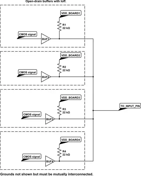
I have multiple IDENTICAL boards of which I plan to 'OR' the signal pins. I know that this can be done using a logic OR IC but that would require a modification on the microcontroller board which I cannot do. The modification must be made on the slave boards, and the slave boards must be identical. Any modification on any of the boards will also be present on the others. I plan the boards to be stacked on top of each other.

enter image description here

What happens with the configuration above is that none of the board can change states. The board is high by default, so when one board tries to go low the line will still be pulled up because of the other boards.

Is this possible?

I was thinking along the lines of something like this, but I dont know if it can actually pull close to 0 because of the diodes:

enter image description here

ocrdu
  • 9,195
  • 22
  • 32
  • 42
DrakeJest
  • 887
  • 11
  • 39
  • 1
    do you realize that you have four pullup resistors connected to one input? – jsotola Feb 26 '22 at 20:07
  • @jsotola yes, i am aware, as i have mentioned anything thats on 1 board must also be on the others, hence why the value is so high, so for example im stacking 10 of them the pullup equivalent would be 10k still. – DrakeJest Feb 26 '22 at 20:23
  • 3
    If you are allowed to modify the slave boards, then you should modify them so that instead of using a CMOS push-pull output, they use CMOS open-drain outputs. Then you don't need the diodes. You would still use the pullups. – user57037 Feb 26 '22 at 20:58
  • I dunno how you do it, but the approach that seems obvious from here is to use a device from the 74LS (or HC) families. I mean, you want to 'OR' 4 signals together, so why not just use a 74LS32? https://www.futurlec.com/74LS/74LS32.shtml – enhzflep Feb 26 '22 at 21:26
  • 1
    @enhzflep OP specifically said they don't want to do that. Also, even if they did, it would require a 4 input or gate, not a quad two input or gate. – user57037 Feb 26 '22 at 22:41
  • For a retrofit, you can also connect the resistors in parallel with the diodes. Depending on your connections, this may be possible to do without modification to any PCB. – jpa Feb 27 '22 at 12:19

5 Answers5

9

schematic

simulate this circuit – Schematic created using CircuitLab

Instead of a diode, put an open-drain buffer on each slave board. Put a pullup on the output of each buffer. The diode thing could work but there are some things to watch out for.

  1. The diode will prevent the signal from being pulled all the way to ground. This reduces noise margin at the input.

  2. If any slave board is powered off, there is a good chance that the powered off board will pull the output low.

This is why I recommend you add a buffer to each slave board instead of a diode. One example part is the TI SN74LVC1G07. However this is just an example. Other vendors make similar parts.

This buffer (and similar parts from other vendors) has the so-called "Ioff" feature which means it will also provide isolation when VDD is not energized, so they will not pull the output down if the board is not powered up.

Please note that the GND from all boards must be connected together. Also, the cap mentioned by Andy is a good idea. The cap can be placed at the output of the buffer.

user57037
  • 29,324
  • 1
  • 30
  • 85
  • The buffer has very robust low-drive capability, so you can use 20k resistors instead. Or even smaller. – user57037 Feb 26 '22 at 21:12
  • how is the buffer orientated>? still the same as the diode? with the output going into the slave board>? can you share a schematic of what you are recommending so i can better understand please. – DrakeJest Feb 26 '22 at 21:59
  • 1
    Added a schematic. Each buffer takes the on-board CMOS signal as its input. The outputs are all wired together and connected to the input pin on the non-slave board. Is there a VCC pin on the non-slave board that you are allowed to connect to? If so, wire that back to each slave and use it as the pull-up VCC for the buffer output. – user57037 Feb 26 '22 at 22:39
  • So the features i have to look for on the buffer is it has to be open drain and a feature of 'Ioff'. How is the capacitor placed? this is not a decoupling capacitor right? i would assume parallel to the resistor? – DrakeJest Feb 27 '22 at 03:00
  • The cap can be parallel to the resistor or at the output of the buffer to ground. – user57037 Feb 27 '22 at 07:06
  • You should use a de-coupling cap also, of course (always with all IC's). – user57037 Feb 27 '22 at 07:08
  • what is the purpose of the cap ? for all i can see is its kind of a deteriment because it lengthen the transistion time of the signal. – DrakeJest Feb 27 '22 at 17:51
  • I like this solution better than the diodes, one last concern though is does it work with most GPIO type (cmos, ttl, etc) – DrakeJest Feb 27 '22 at 17:53
  • The open-drain output of the buffer is comatible with any input that uses the same VCC as the pullup resistor. The inputs to the example TI buffer are CMOS type. But LVTTTL input buffers are available (I think... I haven't actually checked). – user57037 Feb 27 '22 at 18:00
8

I was thinking along the lines of something like this, but I don't know if it can actually pull close to 0 because of the diodes

Yes, you can use diodes like this but I'd give yourself a little bit more headroom and use Schottky diodes; they will drop about 0.3 volts rather than the 0.6 volts for a regular silicon diode.

You don't need all those output resistors either. If you are stacking boards there only needs to be one resistor. However, if you are intent on modifying all slave boards then I'd probably choose something a bit lower than 100 kΩ; maybe 22 kΩ to give a bit more robustness against noise. If you can add a 100 pF output too that adds a little more robustness against noise.

Andy aka
  • 456,226
  • 28
  • 367
  • 807
  • how would the capacitor be placed? parallel to the pullups? Also how about using a paired diode (2 parallel diode in 1 package) would that help even lower the drop to 1.5v ideally? like this one – DrakeJest Feb 26 '22 at 20:28
  • Drop might be even less with those currents, not that it matters too much. – Ralph Feb 26 '22 at 21:29
  • Across the 100 k would be fine. I don't understand about the 1.5 volt comment though @DrakeJest – Andy aka Feb 26 '22 at 21:43
  • misplaced a decimal , 0.15v. – DrakeJest Feb 26 '22 at 21:56
  • @DrakeJest OK I understand. Diodes are non linear and, effectively, 2 parallel diodes might drop 0.2 to 0.25 volts compared to a single diode drop of 0.3 volts. A small gain and probably not that big a deal! – Andy aka Feb 26 '22 at 22:32
2

Yes, the circuit you showed looks all right. The low level will be something like 0.6 V because of the diodes, but that should still be within what is considered logic 0. Datasheet of the microcontroller will tell you the margins of low and high logic input.

Jiří Maier
  • 1,294
  • 3
  • 17
2

Wired logic

Since digital logic has existed, back when people used relays for digital logic, wired logic has been used for exactly this purpose.

With relays, it is possible to use a wired-OR so that whichever switch is active will drive the relay.

For digital logic, it would be possible to use the same kind of wired-OR and drive a signal high or leave it high-impedance, and put a pull-down resistor on the end. Any board taking their signal high will drive the whole thing, and multiple boards going high will simply drive it high more strongly.

This doesn't work very well with digital logic though. With the signal levels used for high and low logic levels, and the input impedance for many logic families (especially older TTL), you'd need a very low pull-down resistor which burns much more power, typically 100R or so.

With that in mind, we usually use a wired-AND where each board drives their output low or leaves it high-impedance, and there's a pull-up resistor on the input. Any output going low takes the line low, and it's only if all lines are high-impedance that the input is pulled high. This can use a much higher pull-up resistor, normally 1K or more, which burns less power.

You then just need to change OR to AND. Fortunately we have De Morgan's Theorem for that, so we just need to put an inverter on each board and another inverter on the input.

Graham
  • 6,150
  • 13
  • 20
1

Assuming what you’re looking for is an active-low OR, your diode solution is ok if you use Schottky diodes with a lower forward voltage drop (e.g., BAT54, Vf = 0.3V.) This will give a valid low for just about any logic type.

You only need one pull-up, at the receiver board (make it about 1.5k) but it’s useful to have weak pull-ups (10k) on each the boards for debugging purposes.

hacktastical
  • 53,912
  • 2
  • 49
  • 152